
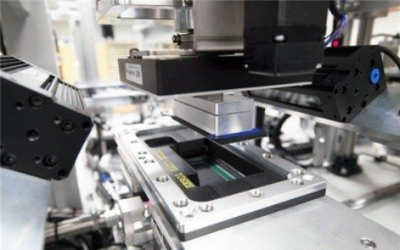
Advanced X-ray Inspection Technology for Complex Multi-layer Printed Circuit Board Assembly Products
X-ray inspection enables non-destructive detection of hidden PCBA defects like BGA voids/cracks, crucial for high-reliability electronics.
Get Your PCB Quote!
Table of Contents

Over the past decade or so, PCBs or printed circuit boards have become extremely complex. They now have high layer counts and very high component density, and their wiring is now more complex. This not only makes defect detection increasingly important, but also makes the effectiveness of overall quality control more difficult. Traditionally, PCB manufacturers and assemblers relied on methods using vision tools, then moved to manual microscope methods, and then to AOI or automated optical inspection. However, with the increasing trend of hidden solder joints, etc. in PCBAs (fan-out, capillary flow), these traditional inspection methods are far from being as effective as they should be.
1. What is X-ray Inspection of PCBA?
X-ray inspection of PCBA is a technology that uses the penetration of X-rays to perform non-destructive testing of the internal structure of circuit board assemblies. It mainly solves the problem of hidden solder joints and internal defects that cannot be observed by traditional optical means.
1.1 Basic Principle of X-ray Inspection
Penetration Imaging: When X-rays penetrate PCBA, materials of different densities/thicknesses absorb the rays to different degrees (such as strong absorption of solder in bright areas and weak absorption of plastic in dark areas). The detector generates a grayscale contrast image to visualize the internal structure.
Defect Identification: Defects such as voids and cracks appear bright white because there is no material to block the rays. Welding problems such as cold solder joints and short circuits are revealed by density differences.
1.2 Core Detection Methods of X-ray Inspection
1) Use a Systematic Process to Improve the Detection Rate:
”Three plus one” layered detection method (applicable to 2D/3D systems):
Global Scanning: Rapidly screen the overall abnormal area.
Local Magnification: Focus on the suspicious point with high magnification for analysis.
Tilt Imaging: Confirm defects (such as BGA cold solder joints) by shooting at multiple angles.
BGA Special Inspection: Actively check for hidden defects such as the pillow effect on ball grid array devices.
2) Technology Evolution: From 2D plane inspection to 3D layered scanning (AXI technology), to achieve three-dimensional structure reconstruction of solder joints.
1.3 Application Scope of X-ray Inspection
Soldering Quality: Solder joint integrity, solder paste filling, bridging defects.
Component Status: Positioning offset, pin deformation, internal cracks.
Structural Analysis: PCB inner layer copper foil connection, via quality, interlayer alignment.
High-density Assembly: Necessary detection means for miniaturized, multi-pin devices (such as CSP, flip chip).
2. Why do We Need to Perform X-ray Inspection on PCBA?
X-ray inspection of PCBA (printed circuit board assembly) is a key link to ensure the quality and reliability of electronic products. Solving the quality control problem of “invisible solder joints” of PCBA through imaging of material density differences has become one of the standard processes for high-reliability electronic manufacturing.
Compared with traditional detection methods, X-ray detection has the following significant advantages:
1) Detect Internal Defects that are Invisible to the Naked Eye
Identification of Hidden Solder Joint Defects: The welding quality of bottom solder joint devices such as BGA (ball grid array) and QFN (quad flat no-lead package) cannot be observed by the naked eye or AOI (automatic optical inspection). X-rays can penetrate the packaging layer and accurately detect internal welding defects such as empty solder joints, cold solder joints, bridging tin, and bubbles.
Structural Defect Detection: It can identify hidden dangers that cannot be detected by the naked eye, such as broken PCB inner layer traces, delamination, microcracks, and abnormal internal structure of components.
2) Improve Product Reliability and Safety
Prevent Functional Failure: Welding defects can easily lead to circuit disconnection or short circuits in extreme environments such as high temperature and vibration. X-ray inspection can intercept such problems before leaving the factory to avoid failure of equipment during operation.
Compliance Requirements in Key Areas: High-risk industries such as automotive electronics, medical equipment, and the military industry have strict requirements on PCBA reliability. X-ray inspection is a mandatory means to meet industry safety standards.
3) Reduce Production Costs and Risks
Reduce Rework Costs: Early detection of defects can avoid batch rework or scrapping. Especially for high-value PCBA, the cost of a single inspection is much lower than the loss of after-sales recall.
Avoid Brand Reputation Risks: Problem products entering the market may cause after-sales disputes and brand trust crises. X-ray inspection is the last line of defense for quality.
4) Powerful Technical Advantages of X-ray Inspection
Non-destructive Testing: Without disassembly or contact with PCBA, X-rays will not damage the PCBA structure and components, maintaining product integrity.
High Precision and Coverage: It can detect more than 98% of hidden solder joint defects (such as BGA and CSP), which is much higher than the coverage of manual or AOI.
Support Complex Design: It is suitable for quality inspection requirements of advanced packaging processes such as high-density interconnect (HDI) boards and fine-pitch components.
5) Industry Application Examples of X-ray Inspection
BGA Welding Quality Assurance: X-rays can intuitively display solder ball size, position offset, and welding integrity, accurately identify false soldering, short circuits, solder ball missing, solder ball offset, voids, tin slag residue, etc., to ensure the reliability of electrical connections in high-density packaging.
3D AXI Technology Application: Automated X-ray inspection (AXI) combined with three-dimensional imaging can accurately locate defects and generate repair guidance reports, greatly improving detection efficiency.
3. How to Perform an X-ray Inspection on PCBA?
1) Inspection Process
Global Scanning
Place the PCBA on the stage, and generate a basic image by X-ray penetrating the overall structure to preliminarily screen the PCB substrate, component layout, and obvious welding defects.
Local Magnification Analysis
Magnify the image (usually 500-2000 times) for suspected areas (such as BGA/QFN solder joints, high-density areas), and observe the solder joint morphology, tin distribution, and connection status.
Multi-angle Tilt Imaging
Rotate the stage (±45°~60°) to confirm three-dimensional structural defects such as cold solder joints, cracks, or pillow effects (Head-in-Pillow) through a three-dimensional perspective.
Quantitative Evaluation of Defects
Measure parameters such as solder joint grayscale value (high brightness in the void area), solder ball diameter deviation (>20% is considered abnormal), and void rate (industry standard is usually <25%).
2) Core Detection Technology
Grayscale Contrast Principle
High-density materials (such as solder) absorb more X-rays, and the image is dark;
Low-density areas (voids/cracks) have high penetration rates, and the image is bright white.
3D-CT Tomography
Through 360°rotation scanning, the three-dimensional model is reconstructed to accurately locate hidden defects such as interlayer short circuits and copper hole fractures.
Automatic Defect Identification (AXI)
The algorithm automatically marks faults such as solder joint bridging, missing parts, and offset. Typical applications include BGA solder ball array analysis.
3) Key Defect Detection Capabilities
| Defect Types | X-ray Image Features | Common Locations |
| Solder Voids | Irregular Bright and White Spots | Inside BGA Solder Balls |
| Pseudo Soldering/Cold welding | Blurred Solder Joint Edges, Uneven Grayscale | QFN Pins, High-power Devices |
| Solder Ball Bridging | Gray Ribbon Connection between Adjacent Solder Joints | Fine-pitch IC Pins |
| Poor Tin Penetration | Reduced Solder Joint Volume, Shrinked Edges | Through-hole Devices |
| Cracks Inside Components | Linear Dark Lines Running Through Devices | MLCC Capacitors, Chip Packaging |
4) Precautions
Projection Misjudgment Avoidance: Tilt observation to avoid component overlap interference (such as side view confirmation of solder joints under the shielding cover).
Resolution Requirements: ≤1μm resolution equipment is required to detect 01005 components or 0.3mm BGA.
Limited Scenarios: The internal structure penetration effect of plastic packaged components is limited, and it needs to be verified with slice analysis.
Modern AXI systems (such as 3D-CT) have realized automated processes, and the single-board inspection time can be controlled within 3-5 minutes, greatly improving the quality inspection efficiency of high-density PCBA.
4. Limitations of X-ray Inspection
Although X-ray inspection of PCBA has significant advantages in defect detection, it still has the following limitations:
1) Equipment and Technology Limitations
Limited Material Penetration Capability: High-density or overly thick materials (such as the inner metal of multilayer boards and large metal shielding covers) will excessively absorb X-rays, resulting in blurred imaging or inability to clearly present the internal structure.
Difficulty in Identifying Small Defects: For defects such as micron-level cracks, tiny voids, or extremely fine open circuits, 2D X-rays may miss detection due to insufficient resolution, and require higher-precision 3D tomography technology.
Limitations in Complex Structure Detection: Complex three-dimensional structures such as stacked packages (PoP) and densely pinned components require multi-angle tilt scanning, which takes a long time and may still have blind spots.
Relatively Slow Detection Speed: Compared with AOI (automatic optical inspection), X-ray scanning and image reconstruction take longer and are difficult to meet the needs of high-speed production lines.
2) Operation and Cost Limitations
High Equipment Cost: The price of high-end 3D X-ray equipment is much higher than that of conventional inspection equipment, and small and medium-sized enterprises are under great investment pressure.
High Threshold for Professional Operation: Experienced operators are required to adjust parameters (such as voltage and focal length), analyze images, and identify defect morphology.
Radiation Safety Protection Requirements: Shielding facilities and protective equipment are required, which increases space planning and safety management costs.
3) Limited Detection Capabilities
Unable to Detect Electrical Performance Defects: For example, electrical parameter drift, signal integrity, and other problems, X-rays can only observe physical structures and need to be combined with ICT (online testing) or functional testing.
Difficult to Quantify Solder Joint Quality: Defects such as solder joint voids and bridges can be found, but quantitative evaluations such as void rate and wetting degree need to rely on algorithm assistance, and the accuracy is affected by image quality.
Insufficient Identification of Contaminants: Non-metallic materials such as flux residues and ion contamination have weak absorption of X-rays and are difficult to image.
4) Special Scene Restrictions
Flexible Circuit Board (FPC) Detection Challenges: Flexible boards are easy to deform, and special fixtures are required for fixing and scanning. In addition, thin-layer materials have low contrast, making defect identification difficult.
Recommendation: X-ray inspection is the core means of PCBA internal defect analysis, but it needs to be combined with AOI (surface defects), ICT (electrical performance), and functional testing to form a complete quality inspection closed loop. For high-reliability fields (such as aerospace and medical), it is recommended to adopt a “2D initial screening + 3D precise scanning” stratification strategy to balance efficiency and accuracy.
5. X-ray Inspection FAQs
Yes. But it is particularly useful for inspecting circuit boards with dense components, including BGA and other packages with solder joints located under their bodies. They can also be used to inspect multi-layer circuit boards with complex internal circuits.
Many types of defects can be found through X-ray inspection, such as solder joint defects, component placement errors, damaged or broken components, foreign debris, internal cracks, delamination, voids, solder bridges, insufficient solder, and more.
Although AOI is cheaper, it has serious limitations, especially for multi-layer circuit boards with components such as BGA, CSP, DFN, QFN, etc. AOI uses visible light for inspection and cannot detect defects hidden under the body of the component and on the top surface of the circuit board. X-rays have stronger penetration and allow you to see the internal structure and defects more deeply.
Yes. By revealing detailed internal structures, X-ray inspection can help rework and repair circuit boards.
When choosing the type of PCB X-ray inspection system, manufacturers must consider its functions (magnification and resolution) and the technologies they support (2D, 3D, CT). In addition, they should also consider its speed and throughput, and whether it is easy to integrate into the existing processes in the manufacturing configuration.
6. Summary
X-ray inspection solves the detection problem of hidden solder joints and microscopic defects by looking through the internal structure of PCBA. It is an irreplaceable means to improve product reliability, reduce risks, and meet high-end industry standards. Especially under the trend of integrated circuit miniaturization, its technological advantages have further strengthened its core position in electronic manufacturing.
In terms of PCBA quality control, our company adheres to the concept of “quality excellence, service first”, and strictly controls every production link, from raw material procurement to finished product delivery, all in accordance with high standards. At the same time, we continuously optimize production processes, reduce comprehensive costs, and strive to bring customers a more cost-effective product experience. In addition, we are well aware that high-quality service is the key to winning customer trust, so we have established a full-process service system covering pre-sales consultation, sample testing, installation and commissioning, and after-sales maintenance so that customers can truly buy and use with confidence. Welcome to send us Gerber files and BOM lists for PCBA quotation!
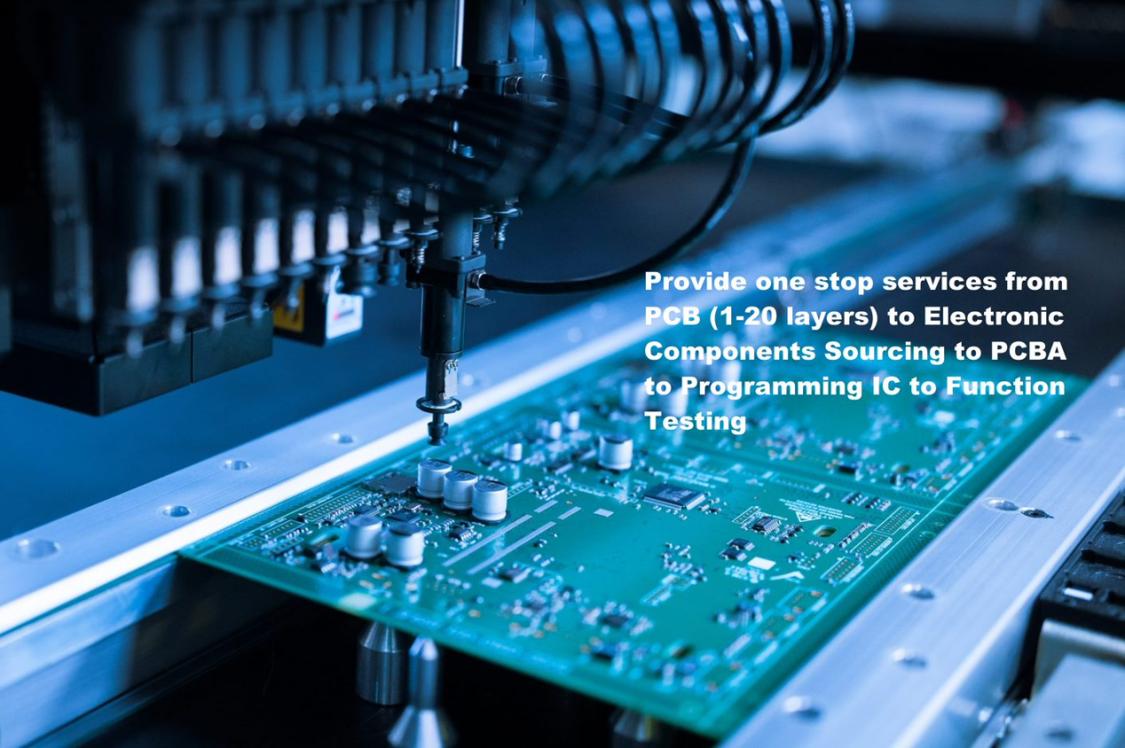
Table of Contents

Get Your PCB Quote!


