
How to Choose the Thickness of standard pcb?
Standard PCB thickness ranges from 0.062 to 0.0633 inches (1.57mm).This thickness is the industry standard. but factors like copper weight, layers,and materials.
Get Your PCB Quote!
Table of Contents
First, in the world of electronic products, the PCB is often referred to as the “heart”, is often called the most important component. It connects all the components together, making board thickness a crucial parameter. The thickness of the board directly impacts the final product’s performance, stability, and reliability.
Various factors influence the process of choosing PCB thickness, including product application scenarios and board materials. These factors must be considered in full when selecting a PCB’s thickness.
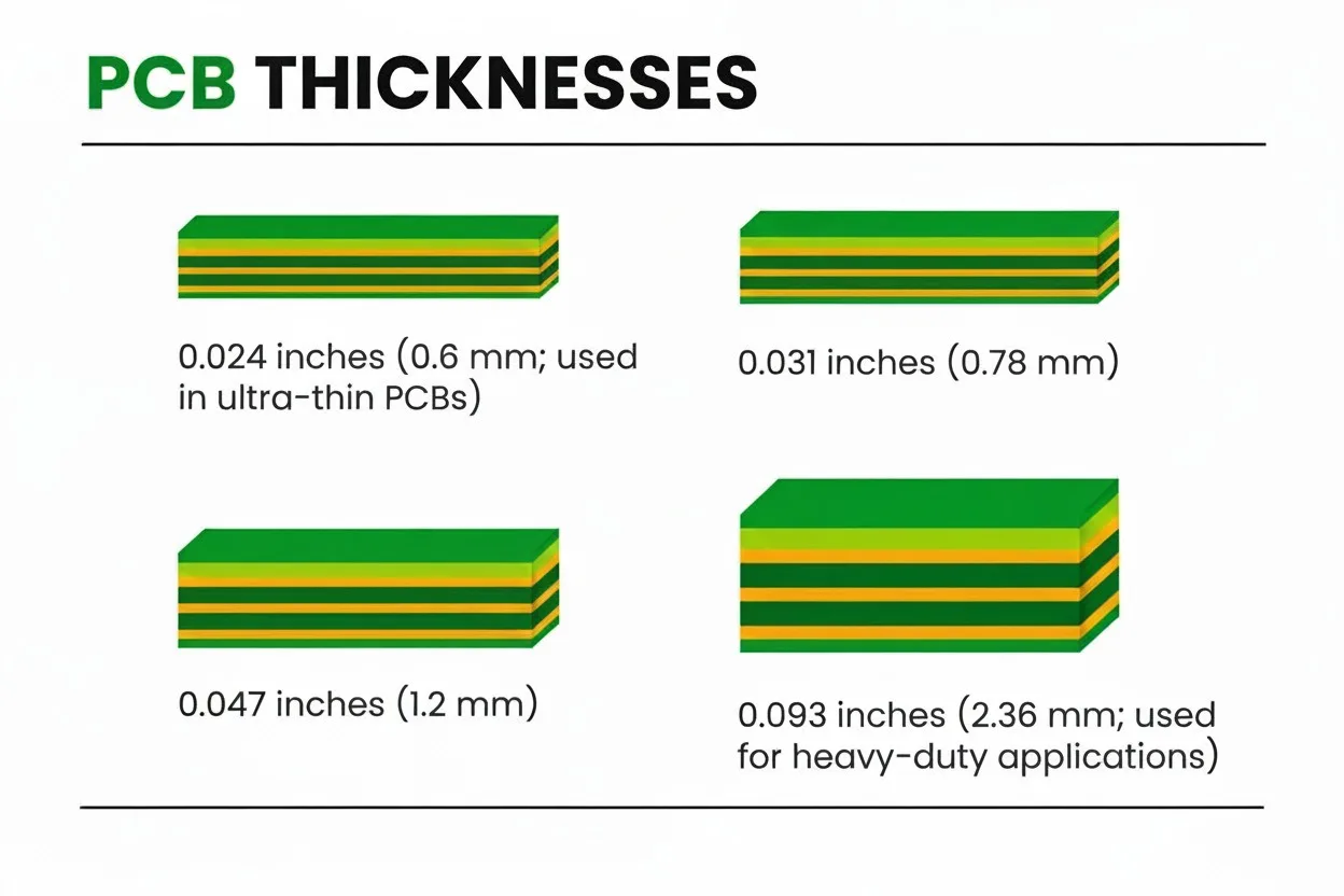
Standard PCB thickness ranges from 0.062 to 0.0633 inches (1.57mm). This thickness is the industry standard. Other popular thicknesses are:
- 024 inches (0.6 mm; used in ultra-thin PCBs)
- 031 inches (0.78 mm)
- 047 inches (1.2 mm)
- 093 inches (2.36 mm; used for heavy-duty applications)
1. PCB panel sizes
Panel Sizes
Panels of PCBs can be produced to make the most efficient use possible of laminate materials. Panels are typically 18″ x 24, which provides a 16″ x 22, usable surface. Standard panel sizes include the following:
- 21” x 24”
- 24” x 32”
- 24” x 30”
- 16” x 18”
The importance of panel sizes
PCB designers must understand the optimal panel size to optimize material use. Due to the need for specialized tools, using larger panel sizes can limit the number of fabricators. Explore the benefits of PCB panels to reduce manufacturing costs and streamline production.
How to Measure PCB Thickness?
PCB is measured with precise tools and techniques, including:
Micrometer: By physically touching the PCB, this instrument offers incredibly precise measurements. It is frequently used to assess the thickness of PCBs on the spot.
Calipers: These offer a rapid and reasonably accurate way to measure the thickness of a PCB. More accurate measurements and easy reading are provided by digital calipers.
Non-Contact Methods: Sophisticated methods, such as optical profilers and laser micrometers, measure thickness without coming into contact with the PCB. For flexible or sensitive PCB boards, this is helpful.
2. What factors influence PCB thickness?
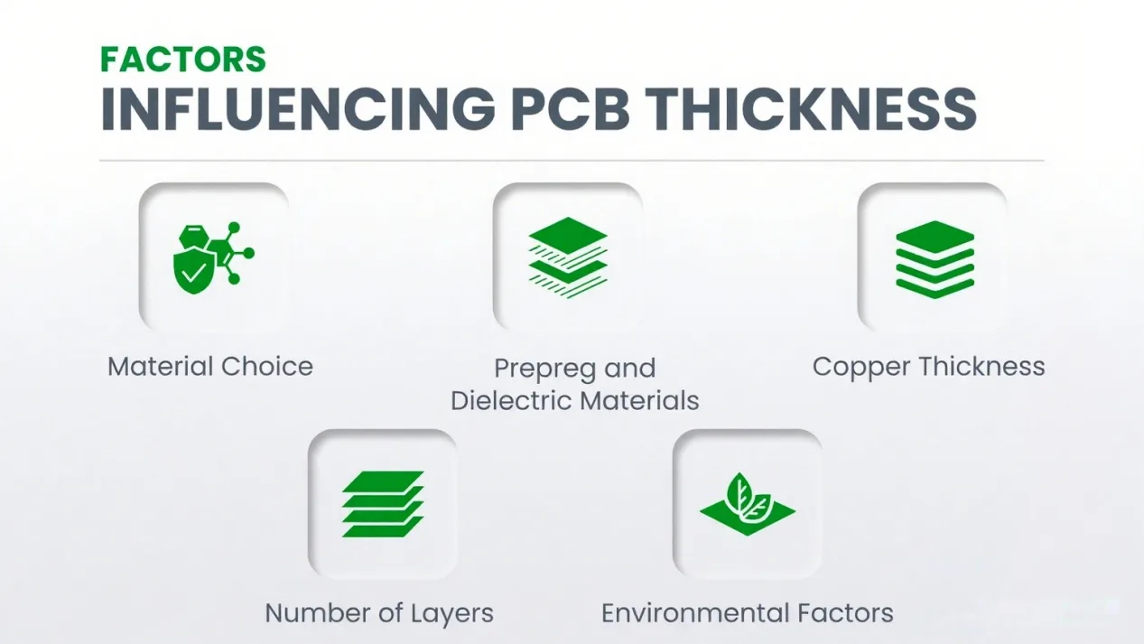
A number of factors can have a significant impact on the thickness of circuit boards, affecting their design, performance, and reliability.
2.1 Material Selection
The thickness of common substrate materials such as FR-4 can range from 0.2 mm up to 3.2 mm. Circuit board materials are chosen based on factors such as thermal and mechanical properties.
2.2 Copper Thickness
Copper thickness is a factor in determining the PCB’s thermal performance and current carrying capacity. Copper thicknesses are typically between 1.4 mm and 2.8mm. Higher thicknesses may be used for applications requiring high power or better heat dissipation.
Also, the thickness of copper is usually measured in ounces/square foot. Copper thicknesses are usually 0.5 oz., 1 oz., and 2 oz. Learn more about the different weights of copper and how they impact PCB performance and design.
2.3 Prepregs and Dielectric Materials
The dielectric material or insulating layer is used between copper layers on multilayer PCBs. Materials ranging from 0.1 to 0.4mm thick are used. The dielectric material used on the PCB can affect its impedance, thermal expansion, and signal speed. Consider polyimide PCBs for demanding applications such as high-temperature and high-frequency designs. They are known for their superior electrical and thermal properties.
2.4 Number of Layers
Multilayer PCBs are typically thicker than 1.6mm. Single-layer PCBs have a thickness of around 1.6mm. The thickness of multilayer PCBs will also be determined by the number and type of conductive layers.
2.5 Environmental Factors
Thick PCBs, with their superior durability and reliability, are recommended in harsh environments such as those with high humidity or temperatures. Thick boards are better at thermal management and mechanical resistance, which makes them ideal for industries such as automotive, aerospace, and industrial control.
3. Why does PCB thickness matter in design?
The thickness of the printed circuit board can affect its performance and durability. Each project is different and therefore requires different PCBs. By choosing the correct thickness, the PCB will be able to handle the electrical and mechanical demands as well as the thermal requirements of the application. Why is it important?
3.1 Electrical Performance
The thickness of the PCB affects its electrical properties, such as impedance and signal integrity. It also influences the current carrying capacity. Thick boards can handle higher current loads. They can also reduce the resistance in the circuit to improve performance.
Signals can be transmitted with no distortion when the thickness is correct. This is important for high frequency applications such as RF and Microwave circuits. Explore PCB transmission lines to learn more about the relationship between trace thickness and signal transmission.
3.2 Mechanical Stability
The rigidity of thicker boards is greater, and they are less likely to bend or warp. This rigidity comes in handy for boards that will be exposed to mechanical stress and vibrations, such as those used in industrial or automotive applications. Learn more about rigid-flex PCBs for designs that need both flexibility and strength. It combines adaptability with stability to meet complex requirements.
3.3 Thermal Management
Thick boards are better able to dissipate the heat, and this is essential for high-power applications. Heat dissipation is important to prevent overheating of components and prolong their lifespan. Thermal conductivity can be improved by using thicker copper layers on the PCB. This ensures that heat is distributed evenly and away from the critical components.
3.4 Assembly of Components
The boards are thicker to support heavier components. They also provide a stronger platform for mounting. This is important for designs that have large or dense components.
Designers must consider the thickness of the board in relation to drilling and etching precision. Overly thick boards may complicate these processes, and can increase manufacturing costs.
4. What is the impact of the thickness of PCBs on manufacturing?
The cost of thicker PCBs is higher because they require more processing time and material. Thinner PCBs can be easier to manufacture and are cheaper, but they may also be more fragile or prone to defects. Here are some limitations that may be caused by PCB thickness.
4.1 Limitations on Drilling Equipment
The equipment that is used to drill the PCBs has limits based on their thickness. To avoid damaging PCB material, drilling must be more precise for thicker boards.
For thicker boards, it can be difficult to control the depth and diameter of holes. Drilling through multiple layers requires more advanced equipment and techniques. The complexity and costs of production will increase.
4.2 Recanalization Techniques
Recanalization involves separating PCBs within a panel. Some of the most common techniques are V-scoring and tab routing. Other methods include punching, water jet cutting, laser cutting and laser cutting.
Each method has advantages and limitations depending on the PCB thickness and design requirements. Laser cutting is more expensive but offers a high-precision edge and is suitable for thicker PCBs.
5. How to choose the right PCB thickness
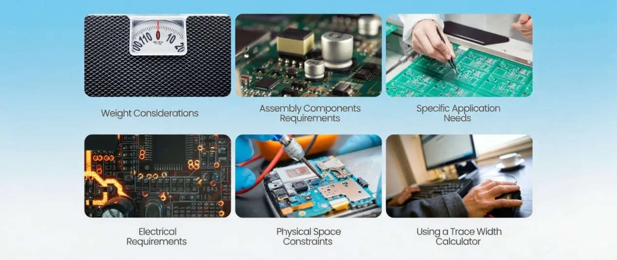
5.1 Weight Considerations
The weight of a PCB directly relates to its thickness. The heavier PCBs can be an issue for portable devices like smartphones, tablets and wearable technologies.
A thicker, heavier PCB is often preferred in applications that require stability and durability, such as automotive or industrial equipment. You should balance the need for durability and strength with the desire to keep the weight of the device manageable.
5.2 Assembly Components Specifications
Some components like heat sinks or large connectors, may require a thicker PCB in order to prevent bending and provide support. The PCB thickness can also affect the soldering procedure. The thickness of the PCB may require more heat to solder, which can affect the soldering materials and techniques.
5.3 Specific application needs
The PCB thickness can be determined by the application. Thinner PCBs are often used in high-frequency RF circuits and microwave circuits to improve performance and reduce signal loss. In contrast, PCBs for power electronics may be thicker in order to support higher current loads or provide better thermal management.
5.4 Electrical requirements
Thick PCBs are able to support higher current capacity, which is important for high-power and power distribution applications. The dielectric layer thickness can also affect the impedance and performance of PCB traces. With a PCB with controlled impedance, you can learn how thickness affects impedance. This will allow for optimal performance.
5.5 Physical Space Constrictions
In order to fit into the small space, compact designs such as smartphones and IoT devices often require thinner PCBs. The PCBs in larger devices can be thicker and may provide benefits for thermal management and strength.
5.6 Using the Trace Width calculator
The trace width calculator can be a useful tool to determine the width of PCB traces according to the amount of current that they must carry and the thickness. The calculator takes into account factors such as the maximum current, temperature rise allowed, PCB material, and properties. You can use a trace calculator to ensure that your PCB traces will handle the current required without breaking or overheating.
6. PCB Thickness management: challenges and solutions
6.1 Warping
When a PCB bends and twists, it can cause connectivity issues and even device failure. Temperature changes, moisture absorption or improper storage can cause this. Manufacturers can:
- Use materials with low thermal expansion coefficients
- Implement balanced copper distribution
- Control the cooling process during manufacturing
6.2 Uneven thickness
Uneven PCB thickness can cause mechanical stress and signal integrity problems. Uneven material distribution or inconsistent lamination pressure can cause this. Solution:
- Ensuring uniform pressure during lamination
- Using high-quality materials with consistent thickness
- Regularly calibrating equipment to maintain precision
6.3 Manufacturing Inconsistencies
Inconsistencies during manufacturing can lead to variations in PCB thickness. This will affect performance and reliability. Equipment wear, variations in the manufacturing process, and human errors are all factors. In order to address the inconsistencies, you can:
- Implement strict quality control measures
- Use automated inspection systems
- Train staff thoroughly to follow standardised procedures
7. Does PCB thickness impact cost?
7.1 Material Costs
The thickness of the PCB will directly impact how much material is needed to make it. The cost of material increases when PCBs are thicker. The cost of thicker boards is also higher because they use more specialised materials.
7.2 Manufacturing Processes
These PCBs are often more complicated to manufacture, requiring multiple lamination cycles and advanced drilling techniques. They may also require additional copper plating layers. These processes require specialised equipment and are time-consuming. This leads to higher production costs.
7.3 Considerations for Design
It can be challenging to design thicker PCBs because they need to have more layers in order for heat to dissipate properly. These complexities may require engineers to spend more time on the design phase, increasing the cost. Testing and validation of complex designs can be required.
7.4 Thermal Management
Thermal management is generally better with thicker PCBs. This is a good thing, but it may also mean that you need to add extra features such as heat sinks and specialised cooling solutions. These extras can raise the price of the final product. High-temperature PCBs can be a crucial solution for applications that require superior thermal performance. They are able to withstand extreme temperatures while still maintaining functionality.
7.5 Application-Specific Needs
Some applications require thicker PCBs in order to meet performance or durability standards. Military, aerospace, and industrial applications, for example, often require thicker PCBs to withstand harsh conditions, which can increase the cost.
7.6 Scale-up Economies
The cost per unit can be reduced by reducing the number of production runs. This will help to spread out the fixed costs that come with a thicker board. Due to increased complexity and materials used, small production runs can result in a higher unit cost.
8. When should custom PCB thickness be considered?
When you need to meet specific performance requirements in your electronic design, consider looking beyond the standard PCB thickness. Here are some situations where custom thickness may be the best option.
8.1 Considerations for PCBs with Custom-Thickness
- High-Power Applications: Thick PCBs can handle high current loads better and are more effective at dissipating the heat. Custom thickness is useful for power electronics, automotive and industrial applications.
- Flexible Circuits: PCBs with a thinner thickness are used for flexible circuits, such as wearables, medical equipment and consumer electronics.
- Signal Integrity: Custom thicknesses can improve signal integrity in circuits, particularly high-frequency ones. Impedance control is crucial for maintaining signal quality, especially in RF and microwave applications.
- Space Constraints: In compact or miniature devices like smartphones and tablet computers, a PCB that is thinner can help save space and create a slimmer profile.
- Mechanical Strength: Thick PCBs have greater mechanical strength and are therefore suitable for applications that require extra support or where there is a need to withstand physical stress, such as aerospace and heavy machinery.
9. How are Custom-Thickness Circuit Boards manufactured?
Several precise steps are involved in the manufacture of custom-thickness boards.
Materials Selection: First, select the base materials (usually FR-4 and copper layers). Materials must be chosen according to desired thickness and electrical properties.
- Lamination Process: Layers of copper and substrate are laminated under pressure and heat. Lamination can be adjusted to achieve a custom thickness by adding or subtracting layers.
- Copper plating: The PCB is copper-plated, and the thickness of the copper can be adjusted according to the design requirements.
- Etching: This step involves removing unwanted copper to create the circuit design. The etching procedure for custom-thickness boards must be controlled carefully to avoid damaging layers or changing the thickness.
- Drilling: Holes are drilled for mounting points and vias. To maintain the accuracy and integrity of the holes, the drilling process should account for custom thickness.
- Silkscreen and Solder Mask: The solder mask protects the PCB from solder bridges and is used to prevent them during component placement. Silkscreen adds labels and markings.
- Final Finishing: Circuit boards are finished with PCB surface finishes such as HASL, ENIG, or OSP. These finishes need to be compatible with custom thicknesses for component soldering.
- Quality Control: Final PCBs are subjected to rigorous testing and inspection in order to verify that they meet all design specifications, including custom thickness.
10. FAQs about standard pcb Thickness
Does PCB thickness affect the performance of electromagnetic interference (EMI)?
Yes. PCB thickness can affect EMI performance. The extra layers of material and PCB thickness can reduce electromagnetic interference and shield the board.
Which are the common applications for ultra-thin PCBs (also known as ultra-thin PCBs)?
Ultra-thin printed circuit boards, usually 0.2 to 0.5mm thick, are used for wearable electronics, flexible displays, medical implant, and compact consumer electronic devices like smartphones and tablet. The thin profile of these PCBs allows them to be bent and folded, which is essential for innovative design.
What is the standard PCB thickness?
The standard thickness of PCBs is typically 1.57 mm (0.06 inches).
PCBs are available in a variety of thicknesses depending on their specific design and application. Although the standard PCB thickness is the most common, it is useful to understand the different PCB thicknesses as well as why they are used instead.
At pcbandassembly, we can design and manufacture custom printed circuit boards of varying dimensions, including custom-designed thicknesses. Whatever your PCB needs, request a PCB quotation today, and we’ll help you create the perfect board.
Table of Contents

Get Your PCB Quote!


