
Master PCB Trace Width: Design, Calculate & Optimize
According to Joule's law, heat is generated when current flows through the resistance of a trace. The core objective of trace width calculation is to ensure that the temperature rise of the trace remains within a controllable range when carrying the maximum current, thereby maintaining the reliability and lifespan of the circuit.
Get Your PCB Quote!
Table of Contents
- 1. Tại sao độ rộng đường dẫn tín hiệu lại quan trọng?
- 2. Dòng điện, điện trở và nhiệt lượng
- 3. Tiêu chuẩn IPC: IPC-2221 so với IPC-2152
- 4. Các yếu tố chính ảnh hưởng đến việc tính toán độ rộng vết in
- 5. Cách tính chiều rộng đường mạch PCB
- 6. Những cân nhắc thực tiễn về thiết kế và các phương pháp tốt nhất
- FAQ
- Tổng kết

1. Why Trace Width is Critical
In the intricate world of printed circuit board (PCB) design, every detail matters. Among the myriad parameters, PCB trace width stands out as one of the most fundamental yet frequently misunderstood elements. It’s not just a setting in your CAD software; it’s a critical determinant of your board’s performance, reliability, and safety. A PCB trace is essentially a copper pathway connecting components, acting as the arteries of your electronic circuit . Its width dictates how much current it can safely carry without overheating, melting, or becoming a literal fuse. An undersized trace can lead to catastrophic board failure, fire hazards, or intermittent operational issues. Conversely, an overly wide trace consumes valuable board real estate, making routing complex and increasing manufacturing costs. Mastering PCB trace width calculation is indispensable for any electronics engineer or hobbyist aiming for professional-grade designs. This guide will walk you through the essential concepts, standards, and calculation methods to ensure your PCB designs are robust and reliable.
2. Current, Resistance, and Heat
At its core, understanding trace width boils down to basic electrical principles. Every PCB trace, regardless of its material, possesses a certain electrical resistance. When an electric current flows through this resistance, it generates heat. This phenomenon is described by Joule’s Law: Power (heat) generated (P) equals the square of the current (I) multiplied by the resistance (R), or P = I²R.
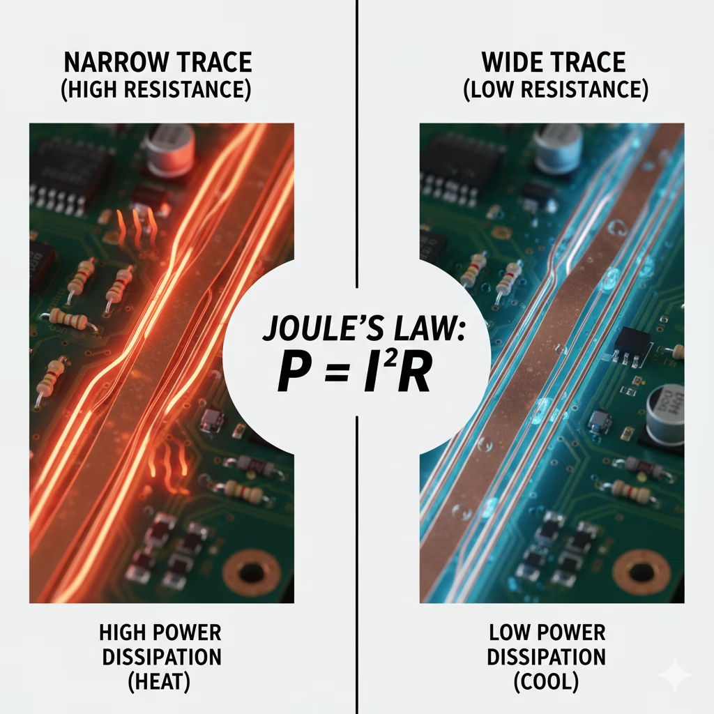
The amount of heat a trace can safely dissipate depends on several factors, including its surface area, proximity to other heat-dissipating components, and the surrounding ambient temperature. If the heat generated exceeds the trace’s ability to dissipate it, its temperature will rise. Excessive temperature rise can lead to:
- Material Degradation:Overheating can damage the copper trace itself, as well as the surrounding dielectric material, leading to delamination or reduced insulation resistance.
- Component Failure:Nearby components can be subjected to temperatures beyond their operating limits, causing premature failure.
- Circuit Instability:Resistance changes with temperature, which can alter signal characteristics and lead to unreliable circuit operation.
- Catastrophic Failure:In extreme cases, a trace can overheat to the point of melting, causing an open circuit – effectively acting as an unintended fuse, but often with hazardous consequences.
Therefore , the primary goal of trace width calculation is to ensure that the trace is wide enough to carry the maximum expected current while keeping the temperature rise within acceptable limits. This directly impacts the board’s reliability and longevity.
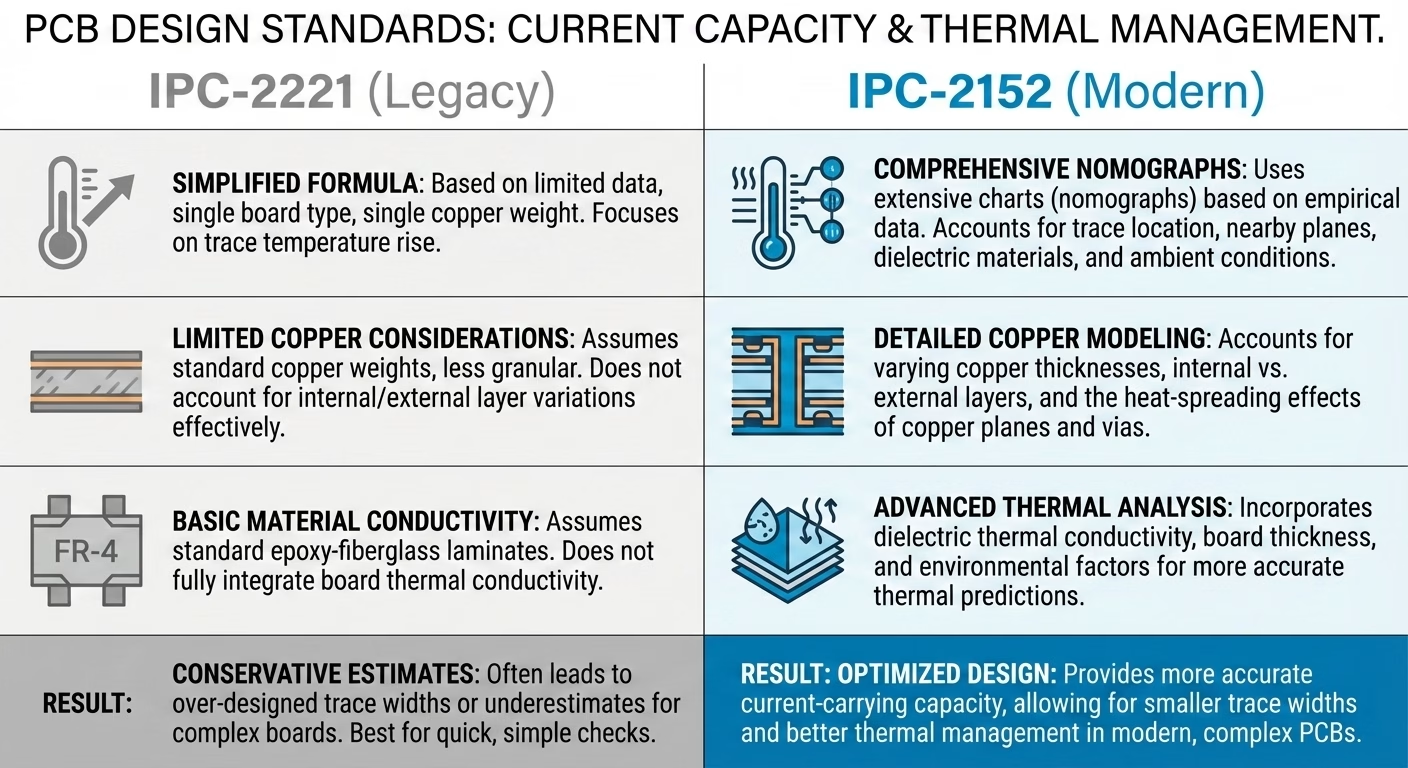
3. IPC Standards: IPC-2221 vs. IPC-2152
To standardize the often complex calculations involved in PCB trace width, the IPC (Association Connecting Electronics Industries) has developed widely adopted guidelines. Two main standards are prominent:
IPC-2221: The Classic Standard
IPC-2221 (Generic Standard on Printed Board Design) is the foundational and most commonly referenced standard for PCB trace width calculations. It provides empirical formulas and charts based on extensive testing, establishing relationships between current, trace width, copper thickness, and temperature rise. Most online PCB trace width calculators, such as those provided by Digi-Key and PCBWay, are based on the IPC-2221 standard formula.
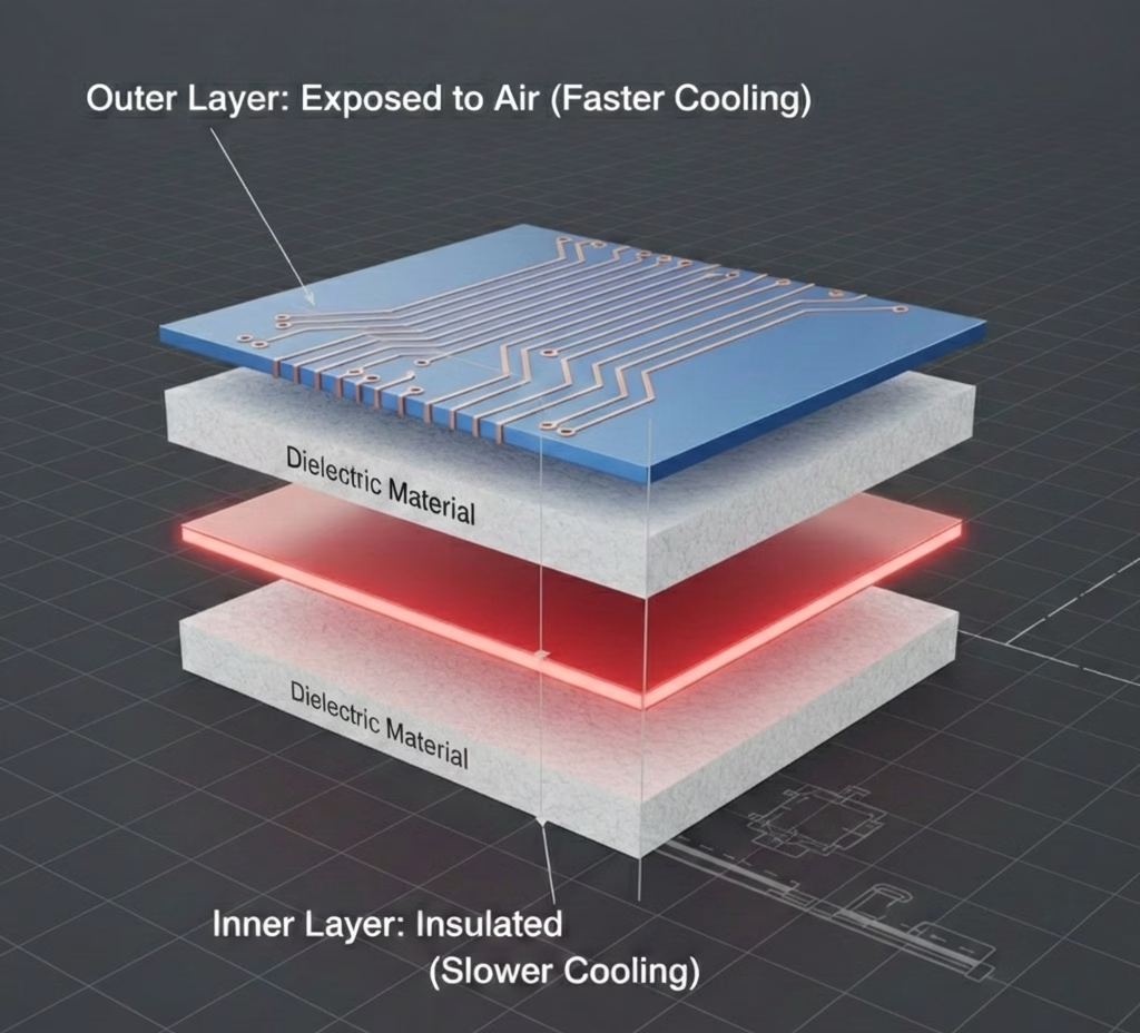
A key distinction in IPC-2221 is the differentiation between external layers (top and bottom) and internal layers. Traces on external layers can dissipate heat more efficiently into the surrounding air, requiring less width for a given current. Internal layers, being encapsulated within the PCB substrate, have poorer heat dissipation and thus require significantly wider traces to handle the same current and achieve the same temperature rise.
IPC-2152: The Advanced Standard
While IPC-2221 remains widely used, IPC-2152 (Standard for Determining Current-Carrying Capacity in Printed Board Design) is a newer, more sophisticated standard. It offers more accurate and empirically derived data, taking into account additional factors like board material, thermal conductivity, and plane layers. IPC-2152 provides more precise estimations, especially for complex, high-power, or high-density designs, making it ideal for professional designs where greater accuracy is paramount Schemalyzer Blog. However, its implementation can be more complex, and many designers still rely on the simpler, yet robust, IPC-2 221 for general purposes.
4. Key Factors Influencing Trace Width Calculations
When calculating the optimal PCB trace width, several interdependent factors come into play . Understanding each of these is crucial for accurate design:
- Current Capacity (Amps):This is arguably the most critical input. The maximum current expected to flow through the trace under normal operating conditions, and ideally, under worst-case scenarios, must be determined. This includes peak currents and surge currents, not just average current.
- Temperature Rise (ΔT or Delta T in °C):This specifies the maximum allowable temperature increase of the trace above the ambient board temperature. A common design goal is often a 10°C rise, but for high-power applications or environments with sensitive components, a lower rise might be necessary. For less critical signals , a higher rise might be acceptable.
- Copper Weight/Thickness (oz):This refers to the thickness of the copper layer on the PCB, measured in ounces per square foot (oz/ft²). Standard copper weights include 0.5 oz, 1 oz, 2 oz, and occasionally 3 oz or more for high-power applications. A thicker copper layer (higher oz) means a larger cross-sectional area for the same trace width , allowing it to carry more current or reduce temperature rise.
Standard PCB Copper Weight Conversions
| Copper Weight (oz) | Thickness (mils) | Thickness (mm) | Thickness (μm) |
| 1.0 oz | 1.37 | 0.0348 | 34.80 |
| 1.5 oz | 2.06 | 0.0522 | 52.20 |
| 2.0 oz | 2.74 | 0.0696 | 69.60 |
| 3.0 oz | 4.11 | 0.1044 | 104.40 |
| 4.0 oz | 5.48 | 0.1392 | 139.20 |
- Layer Type (Internal or External):As discussed with IPC standards, external traces dissipate heat more efficiently into the air, requiring less width than internal traces for the same current.
- Ambient Temperature (°C):The temperature of the environment surrounding the PCB affects the baseline from which the temperature rise is calculated. Higher ambient temperatures mean less room for temperature rise before reaching critical limits.
- Trace Length:While not a primary factor for trace width calculation itself in terms of current capacity, longer traces have higher total resistance and can contribute to voltage drop, which is especially critical for power delivery networks and sensitive analog signals.
5. How to Calculate PCB Trace Width
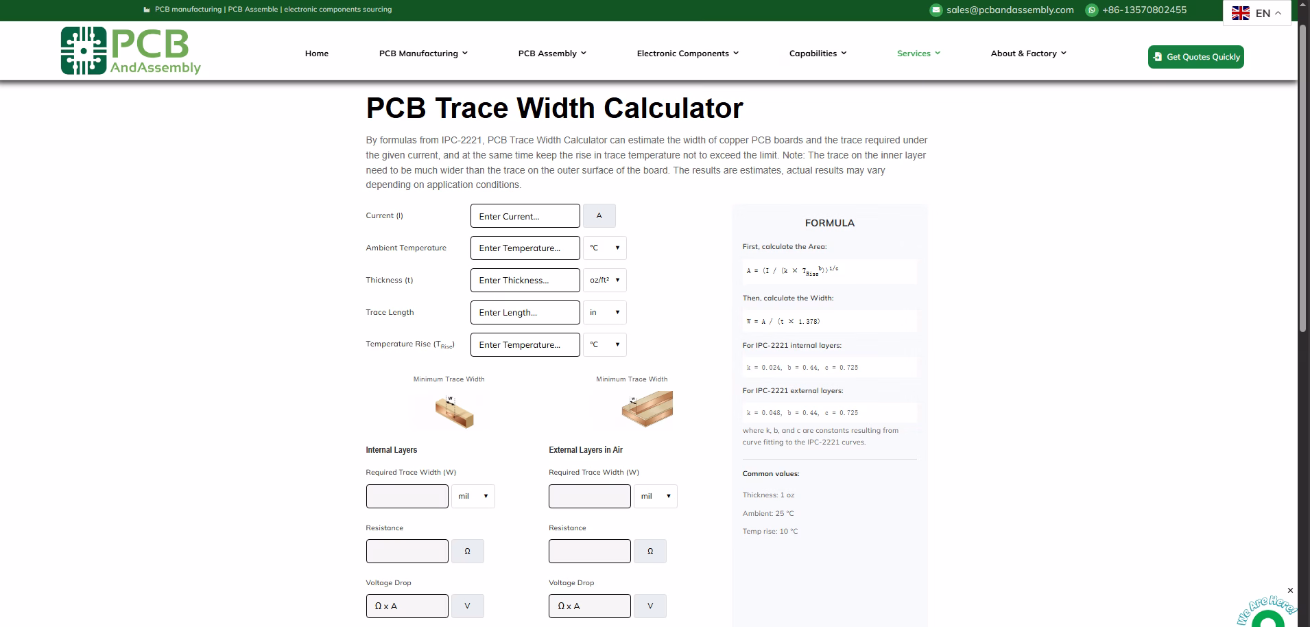
While numerous online calculators simplify the process, understanding the underlying formulas is beneficial. The IPC -2221 standard provides empirical equations that relate current, temperature rise, copper thickness, and trace width. The general process involves calculating the required cross-sectional area first, then deriving the width from that area and the copper thickness.
The formulas, as described by AdvancedPCB, are typically:
- Calculate the Area:
Area[mils^2] = (Current[Amps] / (k * (Temp_Rise[deg. C])^ b))^(1/c)
- Calculate the Width:
Width[mils] = Area[mils^2] / ( Thickness[oz] * 1.378[mils/oz])
Where:
- Currentis in Amps.
- Temp_Riseis the desired temperature rise in degrees Celsius.
- Thicknessis the copper weight in ounces.
- k, b, care constants derived from curve fitting to the IPC-2 221 data.
IPC-2221 Constants:
| Layer Type | k | b | c |
| Internal Layers | 0.024 | 0.44 | 0.725 |
| External Layers | 0.048 | 0.44 | 0.725 |
Notice that the k constant for external layers is double that for internal layers. This reflects the superior heat dissipation of external traces. The conversion factor 1.378 mils /oz is used to convert copper weight (oz) into thickness in mils (1 oz copper is approximately 1.378 mils thick).
Example Calculation (Simplified): Let’s say you need to carry 2 Amps on an external layer, with a maximum temperature rise of 10°C, and using 1 oz copper.
Using the constants for external layers ( k=0.048, b=0.44, c=0.725):
- Calculate Area:
- Area = (2 / (0.048 * (10)^0.44))^(1/0.725)
- Area ≈ 30.5 mils^2( This is an approximation for illustration)
- Calculate Width:
- Width = 30.5 mils^2 / (1 oz * 1.378 mils /oz)
- Width ≈ 22.1 mils
PCBAndAssembly has designed an online PCB Trace Width Calculator that can help you quickly perform calculations.
6. Practical Design Considerations & Best Practices
Beyond the calculations, several practical design rules and best practices will help you create reliable PCBs:
- Always Add a Safety Margin:The calculated trace width provides a theoretical minimum. It’s prudent to add a safety margin by making traces slightly wider than the calculated value, especially for critical power paths or high-current applications. This accounts for manufacturing tolerances, unexpected current spikes, and variations in environmental conditions Schemalyzer Blog .
- Prioritize Internal Layers:As internal layers dissipate heat less effectively, always plan for wider traces on these layers compared to external layers for the same current.
- Thermal Relief Pads:When connecting a trace to a large copper pour or plane (e.g., ground plane, power plane), use thermal relief pads. Directly connecting a trace to a large plane creates a significant thermal sink, making soldering difficult. Thermal reliefs provide a narrower connection, allowing the joint to heat up sufficiently for a good solder connection while still maintaining electrical connectivity.
- Use Copper Pours for High Current:For very high current paths, consider using dedicated copper pours or wide polygons instead of single traces. These significantly increase the cross-sectional area and improve heat dissipation.
- High-Speed Signal Traces:For high-frequency signals, trace width often plays a crucial role in controlling impedance (e .g., 50-ohm or 75-ohm characteristic impedance). In such cases, impedance control might override current capacity as the primary driver for trace width. Consult impedance calculators and stack-up information.
- Voltage Drop Considerations:For sensitive circuits or long power traces, voltage drop (V = I * R) can become an issue. While wider traces reduce resistance, for very long runs, you might need to increase copper weight or use multiple traces in parallel to mitigate voltage drop.
- Manufacturing Capabilities:Be aware of your PCB manufacturer’s minimum trace width and spacing capabilities. Pushing these limits can increase costs or lead to manufacturing defects.
- Sim ulations:For complex or high-power designs, consider using thermal simulation tools to validate your trace width decisions and identify potential hot spots on the board.
FAQ
Question 1: Why do internal traces need to be wider than external traces for the same current?
Answer: Internal traces are surrounded by dielectric material, which acts as a thermal insulator, making heat dissipation less efficient compared to external traces exposed to air. To maintain the same temperature rise, internal traces must have a larger cross-sectional area (i.e., be wider) to manage the heat generated by current flow.
Question 2: What is “copper weight” in PCB design?
Answer: Copper weight refers to the thickness of the copper foil used in PCB manufacturing. It’s measured in ounces per square foot (oz/ft²). For instance, 1 oz copper means that if you spread 1 ounce of copper evenly over 1 square foot, it would form a specific thickness (approximately 1.378 mils or 35 micrometers). Higher copper weight means thicker copper, allowing traces to carry more current or dissipate heat more effectively.
Question 3: What are the consequences of an undersized PCB trace?
Answer: An undersized trace can lead to excessive temperature rise, potentially causing the trace to overheat, melt, and act as an unintended fuse, resulting in circuit failure. This overheating can also damage surrounding components and PCB materials, leading to delamination, reduced board lifespan, or even fire hazards . Signal integrity can also be compromised due to resistance changes with temperature.
Summary
Designing and calculating PCB trace width is a fundamental skill that directly impacts the performance , safety, and longevity of your electronic devices. By understanding the principles of current, resistance, and heat generation, and by adhering to industry standards like IPC-2221, designers can ensure their traces are appropriately sized. Factors such as current capacity, desired temperature rise, copper weight, and layer type (internal vs. external) are critical inputs for accurate calculations. While formulas provide the theoretical basis, readily available online calculators offer a convenient and reliable way to determine optimal trace widths. Always incorporate safety margins and follow best practices to mitigate risks and achieve robust PCB designs that stand the test of time.
Table of Contents
- 1. Tại sao độ rộng đường dẫn tín hiệu lại quan trọng?
- 2. Dòng điện, điện trở và nhiệt lượng
- 3. Tiêu chuẩn IPC: IPC-2221 so với IPC-2152
- 4. Các yếu tố chính ảnh hưởng đến việc tính toán độ rộng vết in
- 5. Cách tính chiều rộng đường mạch PCB
- 6. Những cân nhắc thực tiễn về thiết kế và các phương pháp tốt nhất
- FAQ
- Tổng kết

Get Your PCB Quote!


