
Solve Common PCB Assembly Defects:Soldering,Components & DFM
This guide has explored PCB assembly common problems and solutions such as soldering defects, component-related challenges, and board integrity problems.
Get Your PCB Quote!
Table of Contents

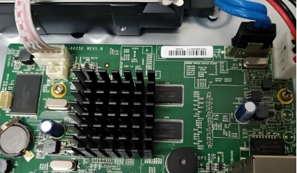
Printed Circuit Board assembly(PCBA) is a critical process in the manufacturing of virtually all electronic devices. From simple gadgets to complex industrial systems, the reliability and performance of an electronic product heavily depend on the quality of its PCB assembly (PCBA). However, the intricate nature of modern electronics, coupled with ever-shrinking component sizes and increasing circuit density, makes PCBA a challenging endeavor prone to various defects.
This comprehensive guide delves into the most common PCB assembly problems, ranging from subtle soldering defects to significant component and board integrity issues. More importantly, it provides actionable solutions and best practices to prevent, identify, and rectify these problems, ensuring higher yield, reduced costs, and superior product reliability. Understanding these challenges and implementing robust quality control measures is paramount for any manufacturer aiming for excellence in electronics production.
1. Understanding PCB Assembly Complexities
The PCB assembly process involves numerous steps, each with its own set of potential pitfalls. These include solder paste printing, component placement, reflow soldering, cleaning, inspection, and testing. A single misstep at any stage can propagate errors, leading to functional failures or reduced lifespan of the final product. The miniaturization trend demands precision in every aspect, making defect prevention even more critical.
2. Common Soldering Defects and Their Solutions
Soldering is the backbone of PCB assembly, creating the electrical and mechanical connections between components and the board. Consequently, PCBA soldering defects are among the most frequently encountered problems. Here are some of the critical ones:
2.1 Insufficient Solder
1) Problem: Insufficient solder occurs when there isn’t enough solder to create a robust electrical or mechanical joint. This can lead to intermittent connections, weak joints, or complete open-circuits.
2) Causes: Inadequate solder paste volume during printing, incorrect stencil aperture design, clogged stencil apertures, improper squeegee pressure, or insufficient reflow temperature causing poor wetting.
3) Solutions:
- Optimize solder paste stencil design for correct aperture size and thickness.
- Regularly clean stencils to prevent clogging.
- Calibrate solder paste printer settings (squeegee speed, pressure, separation speed).
- Ensure proper reflow profile with adequate preheat and peak temperatures.
- Use high-quality solder paste with good rheology.
2.2 Solder Bridging
1) Problem: PCBA bridging refers to the undesirable connection of two or more adjacent pads or leads by excess solder, creating a short circuit.
2) Causes: Excessive solder paste deposition, misaligned components, incorrect stencil design, poor solder paste release from stencil, incorrect reflow profile (e.g., too high temperature or too fast ramp rate leading to solder slump), or contamination.
3) Solutions:
- Optimize stencil design with appropriate aspect ratios and spacing.
- Ensure precise component placement accuracy.
- Adjust reflow profile to prevent solder slump.
- Maintain proper solder paste viscosity and quality.
- Implement rigorous cleaning procedures for boards and stencils.
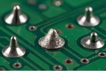
2.3 Solder Balls
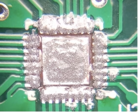
1) Problem: PCBA solder balls are small, spherical solder particles that detach from the main solder joint and adhere to the solder mask or board surface, potentially causing short circuits or cosmetic issues.
2) Causes: Rapid heating during reflow, excessive moisture in solder paste or on the board, improper preheating allowing solvent evaporation too quickly, incorrect stencil design, or inadequate solder mask coverage.
3) Solutions:
- Ensure proper preheat zone in the reflow oven to allow controlled solvent evaporation.
- Store solder paste and PCBboards according to manufacturer guidelines to prevent moisture absorption.
- Optimize reflow profile with a gentler ramp rate.
- Improve solder paste printing quality to avoid excessive paste on non-pad areas.
- Ensure robust solder mask design and application.
2.4 Tombstoning
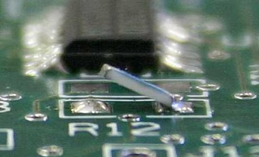
1) Problem: PCBA tombstoning (or Manhattan effect) occurs when a small, two-terminal component (like a resistor or capacitor) stands on one end, resembling a tombstone, due to uneven wetting forces during reflow.
2) Causes: Imbalance in surface tension forces during solder reflow, typically caused by uneven heating, uneven solder paste deposition on pads, or differential pad sizes.
3) Solutions:
- Optimize reflow profile for uniform heating across the board.
- Ensure consistent solder paste volume on both pads of the component.
- Design pads with equal thermal mass and size (DFM consideration).
- Use solder paste with good tack and rheology.
- Place components accurately to minimize offset.
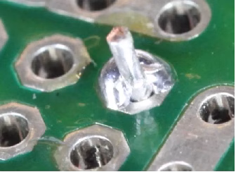
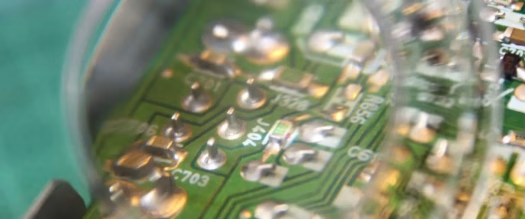
2.5 Cold Solder Joints
1) Problem: A cold solder joint appears dull, grey, and grainy, indicating poor wetting and insufficient heating during the soldering process. Such joints are unreliable and prone to failure.
2) Causes: Insufficient heat applied during soldering (manual or reflow), improper flux activity, or movement of the joint during solidification.
3) Solutions:
- Adjust reflow profile to ensure adequate peak temperature and dwell time above liquidus.
- For manual soldering, ensure proper iron temperature and contact time.
- Use appropriate and fresh flux.
- Ensure components and boards are clean and free of oxidation.
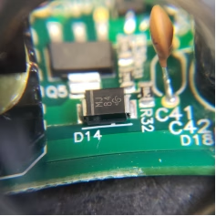
2.6 Lifted Pads
1) Problem: Lifted pads occur when a copper pad detaches from the PCB substrate, often during rework or due to excessive thermal stress.
2) Causes: Overheating during soldering or rework, improper lead-free solder profiles, excessive force during component removal or placement, or poor PCB laminate quality.
3) Solutions:
- Use controlled heating during rework with appropriate tools and temperature settings.
- Optimize reflow profiles to minimize thermal shock.
- Ensure careful handling of PCBs and components.
- Source high-quality PCBs from reputable manufacturers.
3. Component-Related Challenges in PCB Assembly
Beyond soldering, issues related to component handling and placement also contribute significantly to PCB assembly issues.
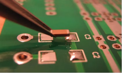
3.1 Component Misalignment
1) Problem: Components are not placed precisely on their intended pads, leading to weak joints, shorts, or open circuits.
2) Causes: Inaccurate pick-and-place machine calibration, worn nozzles, incorrect feeder setup, improper fiducial marks, or board warpage.
3) Solutions:
- Regular calibration and maintenance of pick-and-place equipment.
- Use correct nozzles for specific component sizes.
- Ensure accurate fiducial mark placement on PCBs.
- Implement vision systems for precise component alignment.
3.2 Polarity Errors
1) Problem: Component polarity errors occur when polarized components (e.g., diodes, electrolytic capacitors, ICs) are mounted in the wrong orientation, leading to circuit malfunction or damage.
2) Causes: Human error during manual placement, incorrect component programming in pick-and-place machines, unclear polarity markings on components or PCB silkscreen.
3) Solutions:
- Clear and consistent polarity markings on both components and PCB silkscreen.
- Implement automated optical inspection (AOI) to check polarity.
- Use smart feeders or component verification systems.
- Thorough training for assembly operators.
3.3 Missing or Incorrect Components
1) Problem: A component is either absent from its designated location or an incorrect component is placed.
2) Causes: Feeder issues (empty, jammed), incorrect BOM (Bill of Materials) management, human error, or programming mistakes in the pick-and-place machine.
3) Solutions:
- Robust inventory management and BOM verification.
- Regular feeder maintenance and setup verification.
- Automated component recognition and verification systems.
- AOI checks for component presence and type.
3.4 Damaged Components
1) Problem: Components are physically damaged during handling, placement, or reflow, leading to immediate or latent failures.
2) Causes: Electrostatic discharge (ESD), mechanical stress during handling, excessive heat, improper packaging, or rough treatment.
3) Solutions:
- Implement strict ESD control measures throughout the assembly line.
- Use appropriate handling tools and gentle placement techniques.
- Ensure proper storage and packaging of components.
- Optimize reflow profiles to avoid thermal shock.
4. PCBA Board Integrity and Design-Related Problems
Problems can also stem from the PCB itself or its design, impacting the overall reliability and manufacturability.
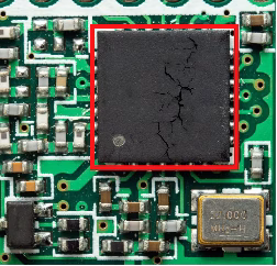
4.1 Warpage and Delamination
1) Problem: PCBA board integrity problems include warpage (bending) and delamination (separation of layers) of the PCB, which can lead to stress on components, solder joint cracking, or even open circuits.
2) Causes: Uneven heating during reflow, improper PCB material selection, mismatched coefficients of thermal expansion (CTE) between materials, improper board design (e.g., uneven copper distribution), or exposure to excessive moisture.
3) Solutions:
- Optimize reflow profiles for gradual and uniform heating and cooling.
- Select PCB materials with appropriate CTE and Tg (glass transition temperature).
- Implement DFM guidelines to ensure balanced copper distribution.
- Store PCBboards in controlled environments to prevent moisture absorption.
- Use support fixtures during reflow for thin or large boards.
4.2 Design for Manufacturability (DFM) Issues
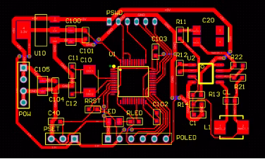
1) Problem: PCBA DFM issues arise when the PCB design does not consider the limitations and best practices of the manufacturing process, making assembly difficult, costly, or defect-prone.
2) Causes: Lack of communication between design and manufacturing teams, designers unfamiliar with assembly constraints, overly dense designs, or non-standard component footprints.
3) Solutions:
- Integrate DFM principles early in the design phase.
- Utilize DFM software tools for design rule checking.
- Establish clear communication channels between designers and manufacturers.
- Standardize component footprints and pad geometries.
- Avoid excessively small features or tight spacing where possible.
4.3 Contamination and Residue
1) Problem: Presence of flux residue, dust, dirt, or other foreign particles on the PCB surface can lead to electrical leakage, corrosion, or poor solder joint quality.
2) Causes: Ineffective cleaning processes, poor quality flux, inadequate handling procedures, or contaminated assembly environment.
3) Solutions:
- Implement robust cleaning processes (e.g., aqueous, solvent cleaning) post-reflow.
- Use no-clean flux sparingly if post-cleaning is not feasible.
- Maintain a clean production environment with proper air filtration.
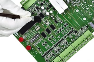
- Ensure operators wear gloves and follow handling protocols.
5. Proactive Measures: PCBA Inspection and Quality Control
Effective inspection and testing are crucial for detecting defects early, preventing costly reworks, and ensuring product reliability. Modern PCBA lines employ a suite of inspection technologies:
| Inspection Method | Description | Primary Benefit |
| Visual Inspection | Manual inspection by trained operators. | Detects obvious defects, quick initial check. |
| Automated Optical Inspection (AOI) | Uses cameras to scan the board for solder defects, missing components, polarity issues , etc. | High speed, consistent defect detection, early detection. |
| X-ray Inspection (AXI) | Penetrates components to inspect hidden solder joints (e.g., BGA, Q FN), voids. | Detects hidden defects, crucial for complex components. |
| In-Circuit Testing (ICT) | Tests individual components and connections for electrical continuity and values. | Verifies component placement and proper connections. |
| Functional Testing (FCT) | Powers up the assembled board and verifies its intended electrical functionality. | Ensures the board operates as designed, detects systemic issues. |
6. Striving for PCB Assembly Zero Defects
Achieving defect-free PCB assembly is an ongoing journey that requires a multi-faceted approach. It combines meticulous design, precise manufacturing processes, quality materials, skilled personnel, and advanced inspection technologies. By proactively addressing common problems like PCBA soldering defects, PCBA component issues, and PCBA board integrity problems, and by emphasizing PCBA DFM issues early in the design cycle, manufacturers can significantly enhance product quality, reduce operational costs, and build a reputation for reliability. Continuous improvement, data analysis, and a commitment to best practices are key to navigating the complexities of modern electronics manufacturing and delivering superior products to the market.
7. PCB Assembly FAQs
Clear polarity markings on both components and PCB silkscreen are essential. Implementing automated optical inspection (AOI) and utilizing smart feeders on pick-and-place machines can further significantly reduce these errors.
Integrating DFM helps prevent PCBA DFM issues by ensuring the design is optimized for manufacturing early on. This leads to higher assembly yields, reduced production costs, faster time-to-market, and improved product reliability by minimizing potential defects.
No. While visual inspection is useful for obvious defects like gross misalignment or large solder bridges, many critical defects like cold solder joints, internal voids in BGA packages, or subtle polarity errors require advanced inspection methods such as AOI, AXI, and ICT.
8. Summary
PCB assembly is a highly complex process central to electronics manufacturing. This guide has explored common issues falling into categories such as soldering defects, component-related challenges, and board integrity problems. We’ve detailed specific issues like insufficient solder, bridging, solder balls, tombstoning, component polarity errors, and DFM issues, along with their root causes and practical solutions. Effective prevention relies on meticulous design (DFM), precise process control, quality materials, and skilled operators. Robust inspection and testing methods, including AOI, AXI, ICT, and FCT, are indispensable for early detection and quality assurance. By addressing these challenges comprehensively, manufacturers can significantly improve PCBA quality, reduce rework, and enhance product reliability.
Table of Contents

Get Your PCB Quote!


