
What is PTH? Why Plated Through Hole Still Matters in PCBA
The guide delves into the essence of PTH technology, exploring its operational principles, advantages, design considerations, and its role in PCB assembly.At PCBAndAssembly, we combine these time-tested PTH techniques with precision manufacturing to ensure your high-reliability projects are built to last.
Get Your PCB Quote!
Table of Contents
In the intricate world of electronics manufacturing, Printed Circuit Board Assembly(PCBA) stands as a foundational process. Among the various methodologies, Plated Through Hole(PTH) technology, though predating Surface Mount Technology (SMT), continues to hold significant relevance. PTH involves inserting component leads through drilled holes in the PCB, which are then soldered to pads on the opposite side. This method creates robust electrical connections and provides superior mechanical stability, making it indispensable for specific applications even in an era dominated by miniaturization.
This comprehensive guide delves into the essence of PTH technology, exploring its operational principles, advantages, crucial design considerations, and its enduring role in modern PCB assembly. Understanding PTH is key to appreciating the diverse landscape of electronic design and manufacturing.
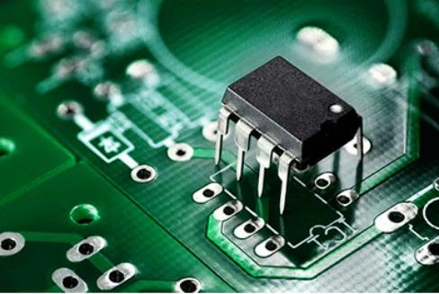
1. Understanding Plated Through Hole(PTH) Technology
Cross-section of PTH PCB
Plated Through Hole(PTH) technology refers to the method of mounting electronic components by inserting their leads through holes drilled in the PCB. These holes are lined with a conductive material, typically copper, which creates an electrical connection between the component lead and the conductive traces on different layers of the board. This plating also serves as a critical pathway for thermal and electrical conductivity.
The primary function of a PTH is to ensure a strong mechanical bond for the component and to establish reliable electrical conductivity across multiple layers of the PCB. Components designed for PTH assembly often have robust leads, making them highly durable and resistant to physical stress.
2. How PTH Assembly Works?
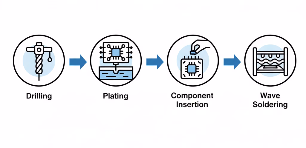
The process of PCB assembly using PTH technology involves several critical steps, ensuring both mechanical integrity and reliable electrical connections:
1) Drilling: Precision drilling creates holes in the PCB substrate where component leads will be inserted. The diameter and position of these holes are crucial for component fit and electrical clearance.
2) Plating: After drilling, the holes undergo a plating process. First, an electroless copper deposition coats the non-conductive hole walls with a thin layer of copper. This is followed by electroplating , which builds up the copper thickness within the hole, connecting the top, bottom, and inner layers of the PCB. This creates what are known as “plated through holes” or “vias”.
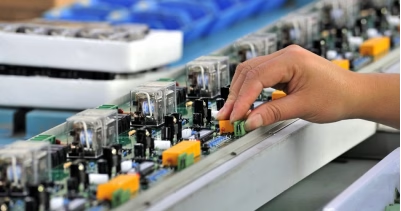
3) Component Insertion: Once the holes are plated and the board fabricated, components with axial or radial leads are manually or automatically inserted into their respective holes. Proper orientation and seating are vital.
4) Soldering: The most common soldering method for PTH components is wave soldering. The populated PCB passes over a wave of molten solder, which flows up into the plated holes by capillary action, creating strong electrical and mechanical bonds between the component leads, the pads, and the hole plating. For sensitive components or specific areas, selective soldering may be used.
5) Inspection and Testing: After soldering, boards undergo thorough inspection (visual, AOI–Automated Optical Inspection) and electrical testing to ensure proper solder joints, component placement, and functionality.
The success of PTH assembly heavily relies on achieving a complete and strong solder fill within the plated holes, encapsulating the component lead and connecting it securely to the board’s conductive layers.
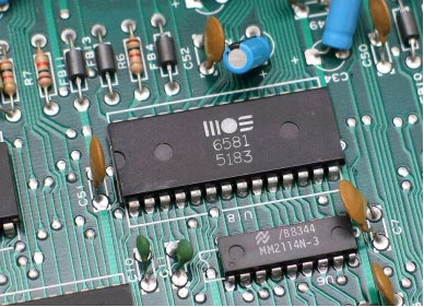
3. Types of PTH Components and Their Applications
While the term “Plated Through Holes” can also refer to vias used solely for inter-layer connectivity, in the context of PCB assembly, PTH primarily refers to the mounting of components with leads. Components compatible with PTH technology generally fall into categories based on their lead structure:
- Axial Lead Components:These components have leads extending from opposite ends, designed to be inserted through holes in a straight line (e.g., resistors, diodes).
- Radial Lead Components:These components have leads extending from one end, typically bent downwards for insertion into holes close together(e.g., electrolytic capacitors, some transistors).
- Through-Hole Connectors:Many connectors, especially those requiring high mechanical strength or frequent mating cycles, utilize PTH technology.
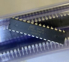
- Integrated Circuits (DIP):Dual In-line Package(DIP) ICs are classic PTH components, though many ICs have transitioned to SMT.
PTH technology is particularly well-suited for applications requiring:
- High Mechanical Strength:Components that need to withstand physical stress, vibration, or frequent connection/disconnection (e.g., large connectors, switches).
- High Power Applications:Components that dissipate significant heat or carry high currents, as PTH provides a larger contact area for heat transfer and robust electrical paths (e.g., power resistors, large capacitors, inductors).
- Prototyping and Manual Assembly:The larger size of PTH components makes them easier to handle, insert, and solder manually, ideal for prototyping or low-volume specialized production.
- Harsh Environments:Their inherent durability makes them suitable for industrial, automotive, and military applications where reliability under extreme conditions is paramount.
4. Advantages of PTH Technology
Despite the advancements in SMT, PTH technology maintains a strong foothold due to its distinct advantages:
- Superior Mechanical Strength:Components inserted through holes and soldered on both sides create a much stronger physical bond with the PCB compared to surface-mounted components. This makes them highly resistant to vibration, shock, and thermal cycling.
- Enhanced Heat Dissipation:The larger physical connection and the ability to route heat through the plated hole and component lead allow for better heat dissipation, especially for high-power components.
- Ease of Manual Assembly and Rework:The larger size of PTH components and their leads simplifies manual handling, inspection, and rework processes. Desoldering and replacing a PTH component is often more straightforward than with tiny SMT parts.
- Reliability in High-Stress Environments:The robust nature of PTH connections makes them ideal for applications exposed to harsh environmental conditions, providing long-term reliability.
- Cost-Effectiveness for Prototyping :For small batches or prototypes, PTH components can be more economical as they often do not require complex pick-and-place machinery.
5. Considerations for PTH Technology
While beneficial, PTH technology also comes with its own set of design and manufacturing considerations:
- Board Space Consumption:PTH components require more board space due to their larger footprint and the need for drilled holes and surrounding pads. This can limit component density, especially in compact designs.
- Higher Drilling Costs:The drilling and plating processes for PTH add to the manufacturing cost, particularly for boards with a high number of through-holes.
- Limited Miniaturization:The inherent size of PTH components restricts their use in highly miniaturized electronic devices, where SMT is often the only viable option.
- Slower Assembly Process:Manual or automated insertion of leads into holes can be slower than the high-speed placement of SMT components. Wave soldering, while efficient, may not be suitable for all component types or board layouts.
- Design Complexity:Proper annular ring design, hole size tolerances, and pad dimensions are critical for robust PTH connections and require careful consideration during PCB design.
Here’s a comparison of key aspects between PTH and SMT:
| Feature | Plated Through Hole(PTH) | Surface Mount Technology(SMT) |
| Mechanical Strength | High (components fixed through holes) | Lower (components soldered to surface pads) |
| Component Density | Lower (requires more board space) | High (smaller components, fewer drilled holes) |
| Assembly Speed | Slower (insertion, then soldering) | Faster (automated pick-and-place) |
| Rework Ease | Generally easier for individual components | Can be more challenging, requires specialized tools |
| Heat Dissipation | Better for large/high-power components | Can be challenging for high-power; thermal vias often used |
| Prototyping | Easier manual assembly | Requires specialized equipment or adapter boards |
6. The Critical Role of Solder Fill
In PTH assembly, the quality of the solder joint within the plated hole, known as “solder fill”, is paramount. Proper solder fill ensures several critical functions:
- Robust Electrical Connection:It establishes a reliable electrical path from the component lead to the plated barrel and, consequently, to all connected layers of the PCB.
- Strong Mechanical Bond:A well -formed solder joint fully encapsulates the component lead within the plated hole, providing significant mechanical strength and stability against vibration and stress.
- Efficient Thermal Transfer:Solder fill aids in dissipating heat from the component, channeling it through the plated hole into the copper planes of the PCB, which is crucial for high-power applications.
Achieving optimal solder fill requires careful control of soldering parameters, including solder temperature, wave height, and board travel speed during wave soldering, or precise control in selective soldering processes. Insufficient solder fill can lead to intermittent connections, premature component failure, and reduced reliability of the overall assembly.
7. PTH vs. SMT: Complementary Technologies
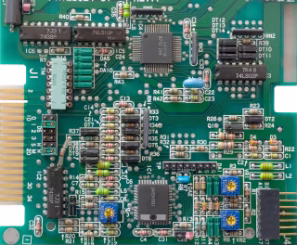
While SMT has become the dominant technology for high-density and miniaturized electronics, it’s crucial to understand that PTH is not obsolete. Instead, PTH and SMT are often complementary, frequently coexisting on the same PCB. Hybrid designs leverage the strengths of both:
- SMT for high-density, low-power digital circuits and smaller components.
- PTH for bulky, high-power, high-stress components like power connectors, large capacitors, transformers, and voltage regulators.
This synergistic approach allows designers to achieve the benefits of miniaturization and high component density with SMT, while still providing the necessary mechanical robustness and thermal management offered by PTH for specific critical components.
8. PTH Technology FAQs
PTH components have leads that pass through drilled, plated holes in the PCB and are soldered on the opposite side, providing strong mechanical and electrical connections. SMT components are soldered directly onto pads on the surface of the PCB, allowing for greater miniaturization and higher component density.
PTH is preferred for components requiring high mechanical strength, excellent heat dissipation (e.g., high-power devices), ease of manual assembly/rework, and reliability in harsh environments, where SMT might not offer sufficient robustness.
Solder fill refers to the molten solder completely filling the plated through-hole around the component lead. It’s crucial for creating a robust electrical connection, a strong mechanical bond, and efficient thermal transfer from the component to the PCB.
Yes, it is very common to create hybrid PCBs that utilize both PTH and SMT components. This approach leverages the strengths of each technology, using SMT for dense, small-signal areas and PTH for robust, high-power, or frequently connected components.
9. Summary
Plated Through Hole(PTH) technology remains a vital method in PCB assembly, recognized for its unparalleled mechanical strength, superior heat dissipation capabilities, and ease of rework. Though it requires more board space and has a slower assembly process compared to Surface Mount Technology(SMT), its advantages in specific applications–such as high-power components, robust connectors, and devices operating in harsh environments-ensure its continued relevance. The meticulous process of drilling, plating, component insertion, and especially proper solder fill, are fundamental to achieving reliable and durable PTH assembly. By understanding the intricacies and appropriate applications of PTH, alongside SMT, engineers can design and manufacture robust electronic products that meet the diverse demands of today’s technological landscape.
Table of Contents

Get Your PCB Quote!


