PCB Manufacturing Assembly: How Printed Circuit Manufacturers Shape the Industry
Get Your PCB Quote!
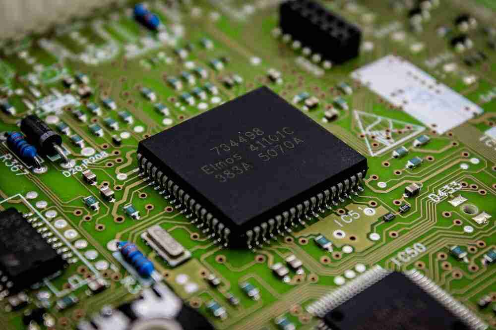
The printed circuit board industry is an essential part of modern electronics because it serves as the base of almost all electronic gadgets. Development of technology increases the PCB complexity, which raises the need for more skilled manufacturers to cope with the increasing market demands. This article meets the expectations of curiosity on how the PCB manufacturing process occurs and how skilled manufacturers contribute to molding an industry that is vital.
What is PCB Manufacturing Assembly?
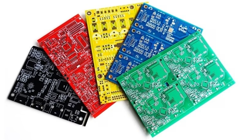
PCB manufacturing assembly is a process that pertains to creating the printed circuit boards applied in a variety of electronic devices. In different stages, the circuit layout needs to be designed until the board is actually constructed. Specialists integrate expertise in electronics, materials, and machinery for this highly segmented process to ensure precision and reliability.
The Importance of Quality in PCB Manufacturing
Without quality control in the production of printed circuit boards-deliberate checking on manufacturing parameters being used during PCB assembly and the testing gone at every production stage, like visual inspection, electrical testing, and performance testing-a single point defect might lead to failure in the final product. Cause-based analysis, in turn, would be more than necessary if PCBs get broken during usage.
Correct position of the components on the pcb is one of the most important part of quality control. This guarantees that all the electrical pathways are not damaged and working. Additionally, a printed circuit manufacturer uses automated optical inspection (AOI) systems to detect any defects in the PCB during production. These systems help catch any issues early on, preventing costly rework later.
Steps Involved in PCB Assembly
To put together a PCB, it is broken down into several stages that require sharp working attention and accuracy. Several steps are outlined below that should be considered to make the entire PCB Assembly process hassle-free:
1. Design and Prototyping
The design phase takes place before some work begins in a physical form. With the use of specialized software, the engineers draft the schematic diagram of the PCB by determining components and their locations on the board.
Prototyping is a stage of due importance because it helps the engineers to test their design before it is turned into a mass production. A step is very important in identifying any design or inefficiencies which will further dilute the product.
2. PCB Fabrication
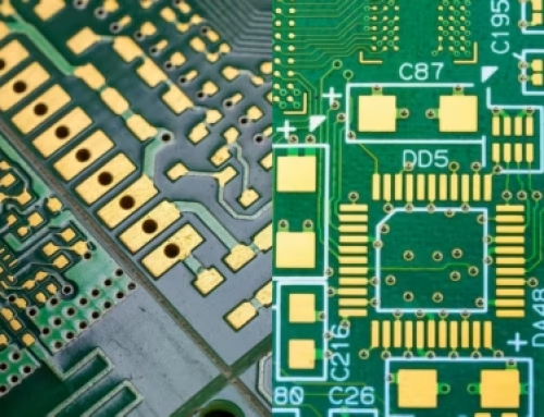
Manufacturing of the physical board comes next – basically at this stage, the copper clad substrate finds itself etched while the excessive copper is removed. That will leave micro-tracks for circuit linking. Holes for component leads and vias for electric signals between layers round up the later.
At times, more complicated boards are needed. These are multi-layers that sandwich layers of boards and interconnect them together. Performance-oriented applications that need high functionality and are compact designs often require such intricate boards.
3. Solder Paste Printing
After a board has been manufactured, solder paste is applied on the PCB. This material consists of tiny metal grains and a flux, which are used to attach the components to the board. For applying solder paste at the exact location of component placements, this process uses a stencil. This is the most important process to bind the components tightly to the board and to withstand upcoming soldering with those components.
4. Component Placement
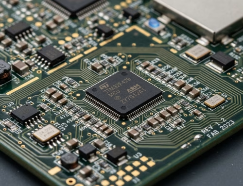
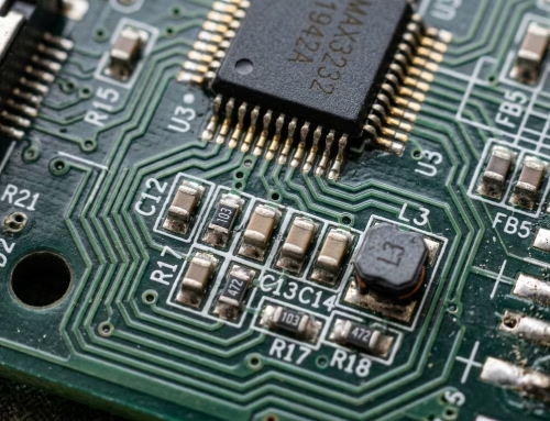
Following the process, the components are mounted in the positions on the PCB where the solder paste is. Automatic machines are used to perform this stage, placing the components onto the PCB. The accurate placement of components is an essential provision as any misalignment may lead to faulty connections or short circuits.
5. Reflow Soldering
The reflow soldering of the board after the components have been installed is next. It implies heating the printed circuit board in a reflow oven so that the solder paste melts and forges a good electrical path between the solder paste and the components against the PCB. Extreme control of temperature is demanded within the oven to avoid overheating, thus damage, to the components.
Typically, a reflow soldering process comes in increments, with the temperature rising slowly, one after the other, to allow the solder to melt so as to form solid joints for electrical connections of devices on board. Afterward, the board is cooled to freeze the stabilizing solid solder connections that have come about.
6. Inspection and Testing
Other than the soldering process, the Printed Circuit Board (PCB) also has to undergo an assessment aimed at verifying the proper positioning and full functionality of all the components. There are different methods that could be used for an assessment, like Automated Optical Inspection (AOI), X-ray, or electrical testing.
AOI techniques are for visual defects like missing or misaligned elements while X-ray is great for inspecting hidden solder joints and into each of the internal layers of a multi-layer circuit board. Electrical testing verifies the working of the PCB through the detection of open circuits and short circuits.
7. Final Assembly and Packaging
Board passed all the inspections and tests; then, the final assemblies will come to place. It refers to the last activity where one attaches on connectors, slots the board into the housing, or the additional modules required for the end product. Finally, the boards are packed and shipped to the particular customers.
The Future of PCB Manufacturing
The future of PCB assembly appears bright as technology continues to develop. There is still scope for far more automated assembly processes, which will consequently reduce the cost for production and improve efficiency. Innovations in material, with flexible PCBs and biodegradable substrates, will allow new things to be done in electronic designs.
Summary
PCB assembly is an utmost stage in the electronics industry because it is instrumental in developing devices that shape our daily lives. From conception to the final assembly, each step in the PCB assembly manufacturing process should be meticulous and thorough for delivering the finest quality. As the demand for such advanced technology grows, so does the demand for highly skilled manufacturers in order to face new challenges.
Get Your PCB Quote!

