PCB Gold Fingers: What They Are, How They Work & Design Rules
Gold fingers are the connector interface between PCBs and edge slots — and getting their plating thickness, chamfer angle, and spacing wrong causes failures. Here's what to know.
Get Your PCB Quote!

Table of Contents
Pcbandassembly manufactures various printed circuit boards for the computerized and mobile world. Most of these PCBs carry signals to and from other devices. For proper functioning of these boards, it is necessary for them to communicate without interruption. Gold fingers on PCBs act as connection points between boards, making this possible. Gold fingers are a huge advancement in the efficient transmission of signals and commands compared to earlier technologies. In a word, Gold fingers make communication between different boards and modules flawless.
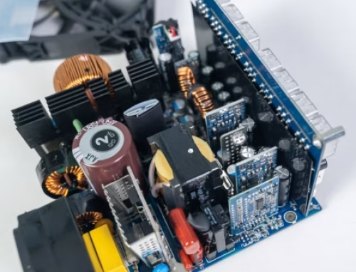
Gold Finger
Printed circuit boards that must communicate with other boards often have gold fingers on their edges. These are multiple gold-plated posts visible along the edge of the board that are used to connect to connectors. For example, auxiliary PCBs, such as graphics cards, have gold fingers that plug into connectors on a computer’s motherboard. Smartphones and smartwatches also have gold fingers on their PCBs, as do many other devices that communicate via digital signals. To achieve a good connection on the edge of a PCB, the plating alloy has a high electrical conductivity.
Types of Goldfinger
PCB manufacturers offer two processes for creating gold fingers on the edge of a board:
Hard gold electroplating — Better suited for boards that are repeatedly plugged in and out. The gold provided is hard and typically 30µ inches thick. It can withstand the wear and tear of repeated use.
ENIG or electroless nickel immersion gold — This gold is much softer and typically 2-5µ inches thick. While this gold is more cost-effective and easier to solder, it cannot withstand the wear and tear of repeated use.
Since signals and power must be transmitted to different boards, they typically pass through various contacts. This means that each contact must have the lowest possible resistance to prevent voltage drops. The gold plating on the fingers ensures that contact resistance remains low.
Gold finger electroplating process
The electroplating process for gold fingers involves many meticulous steps. This ensures that every circuit board on the production line has extremely low resistance when conducting signals and power without any errors. Manufacturers usually follow international electroplating process standards to ensure that each gold finger on the circuit board fits perfectly with the corresponding slot in the connector.
To enable a smooth fit between the fingers and the slots in the connector, each board must pass a series of inspections and tests for defects. Lack of smoothness on the gold plating on a circuit board, or if the gold is not adhering adequately to the board surface, may result in rejection of the board.
In the PCB manufacturing process, the fabricator can complete the plating process only after completing all other activities on the board. Before starting the actual gold plating process, manufacturers will plate a layer of nickel on the copper fingers. Then they apply a gold surface coating. The circuit board is then inspected under a magnifying glass and subjected to adhesion tests.
Using Gold Fingers
Gold fingers are the connection contacts between two PCBs. In addition to providing high conductivity, gold plating protects the communication pins from wear and tear from repeated handling. The strength of hard gold and the extra thickness on the gold fingers allow the circuit boards to be connected, disconnected and reconnected in the socket more than 1000 times without any wear or damage to the fingers.
Gold fingers have many functions. For example, in a computer setting, many peripheral devices can be connected to the computer through various types of gold fingers. Gold fingers are useful in many applications, such as:
• Internal Connections — Sub-boards are usually connected to the main motherboard through various types of female connectors such as AGP, ISA, or PCI. Gold fingers on the PCB interconnect the signals between the sub-board and the motherboard or between the peripherals and the computer.
• Special Adapters — The performance of a personal computer can be enhanced using gold fingers. For example, auxiliary PCBs such as graphics cards and sound cards are connected vertically to the motherboard to provide high-quality graphics or high-fidelity sound. Since users rarely plug and unplug these cards, most use soft gold fingers, which have a longer service life.
• External Connections — Many outer peripherals connect to a personal computer. These include speakers, scanners, monitors, printers, and USB devices. Most of these devices are plugged into various sockets on the computer. The gold fingers on these sockets and devices are often worn out due to frequent plugging and unplugging. Therefore, most of these connectors usually use hard gold fingers.
Any device needs power to operate after being connected to the motherboard. The connector slots on the motherboard usually provide power. Here, the gold fingers also transfer power from the motherboard to the auxiliary board, allowing it to operate perfectly.
Motherboard manufacturers usually provide flexibility through various connector systems, allowing different types of cards to be connected. This allows users to upgrade their computer systems regularly over a few years. Updating a sound card or graphics card requires unplugging the old card and replacing it with a new improved model. During the upgrade process, the gold fingers on the PCB remain universal contacts.
Gold Fingers’ application range is not limited to personal computers. For example, industrial machinery also uses gold fingers as connection contacts. For example, an automobile factory or a stamping plant usually has numerous mechanized equipment with internal cards connected to the main power supply, and gold fingers are used in the process. The industry uses a robotic arm to receive power and control signals through the gold fingers on the card.
Gold Finger Specifications
In order for gold fingers to work properly, manufacturers must follow certain standards during the electroplating process. The design of the PCB must also facilitate proper finger length and alignment. Regardless of the size or purpose of the PCB, some rules that apply to gold finger design are as follows:
√ No PTH or plated through holes near gold fingers.
√ No solder mask or silkscreen near gold fingers.
√ All gold fingers must terminate at the edge in the middle of the board.
Failure to follow the above rules may result in the PCB not being able to be inserted into the motherboard. For example, the daughterboard may not fit properly in the corresponding slot on the motherboard.
Gold has excellent strength and conductivity, which is the main reason why it is used for connecting fingers. Gold allows the fingers to be inserted and ejected hundreds of times without causing the contacts to wear out. Without the protection of gold, copper fingers on a circuit board would easily wear out after a few uses.
Although gold is one of the most expensive and rare metals used for PCB fingers, it provides a necessary function on printed circuit boards. This is due to several factors. The main benefit of the use of gold comes from its high electrical conductivity and its resistance to corrosion. The added strength comes from the application of gold in combination with nickel or cobalt, both of which provide it with the necessary wear resistance during repetitive activities.
IPC has developed production standards for PCB gold fingers, such as IPC A-600 and IPC-6010, which define the chemical composition, thickness, and tape testing for any gold plating process on PCBs.
Gold finger plating restrictions
Electroplated gold fingers must follow certain restrictions. These include:
√ Inner layer copper must not extend to the edge of the PCB. This is to prevent copper exposure during beveling.
√ No SMD parts, plated holes, or pads are allowed within 1 mm of the gold finger.
√ All gold fingers must be less than 40 mm in length.
√ Any gold finger must be at least 0.5 mm away from the PCB outline.
Deviating from the above gold finger spacing requirements may cause the card to malfunction or lose physical strength.
Summary
As technology becomes more and more dependent on gold fingers, Pcbandassembly recommends that gold fingers be plated and tested to the highest standards. This is how we ensure that gold fingers perform at their maximum performance in quality circuit boards.

Get Quote Free