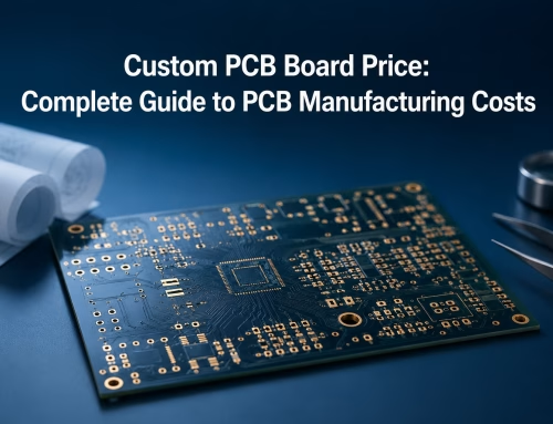
For PCB Engineers or Buyers, How to Save Printed Circuit Board Assembly Costs?
Guide to cutting PCB assembly costs via design optimization, component sourcing, and process efficiency while maintaining quality.
Get Your PCB Quote!

Table of Contents
1.What is PCB Assembly?
PCB assembly (commonly known as PCBA or Printed Circuit Board Assembly) refers to the manufacturing process of installing and soldering electronic components to a printed circuit board (PCB) to form a complete circuit module with specific electrical functions.
1.1 How to Assemble a PCB?
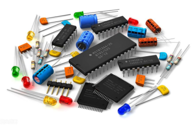
Fix electronic components (resistors, capacitors, chips, etc.) to the pads or through holes of the PCB through soldering technology (such as reflow soldering and wave soldering) to achieve electrical connection.
1.2 What are the Differences between PCB and PCBA?
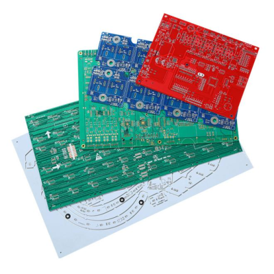
PCB is a “bare board” without components installed, only containing circuit layout; PCBA is a “functionalized circuit board” with component assembly completed.
1.3 What is the Key Technical Process of PCB Assembly?
1) Component Placement
SMT (Surface Mount Technology): Micro components (such as chip resistors and IC chips) are accurately placed on the PCB pads through a placement machine and cured by reflow soldering.
THT (Through Hole Technology): Insert plug-in components with pins (such as electrolytic capacitors and connectors) into PCB through-holes and fix them by wave soldering or manual soldering.
2) Soldering Process
Reflow Soldering: Applicable to SMT components, high-temperature melts solder paste to form solder joints.
Wave Soldering: Applicable to THT components, molten solder surges to solder pins.
3) Inspection and Testing
AOI (Automated Optical Inspection): Scan solder joint quality and identify defects such as cold soldering and offset.
Functional Test (FCT): Power on to verify whether the circuit performance meets the design specifications.
2.Why Should We Reduce the Cost of PCB Assembly?
The PCBA is the “brain” of electronic devices, and almost all electronic products (mobile phones, computers, industrial equipment) rely on it to achieve their functions. However, in order to keep the business profitable, electronic products must be viable, and designers must learn to reduce the cost of PCBA without sacrificing quality and functionality because it is essential to stay competitive. Therefore, PCB designers must balance the skills of creating PCBs from scratch with the knowledge of PCB assembly cost control.
The total cost of PCB assembly can be roughly divided into three parts:
PCB bare board cost (Gerber)
Component procurement cost (BOM)
PCB assembly, testing, and steel stencil cost
The cost of individual components and printed circuit boards is much higher than the cost of PCB assembly and testing. As a PCB engineer or purchaser, he/she can influence the total cost of PCB assembly by choosing components and PCBs wisely, because the latest and most advanced components are bound to be more expensive.
3.How to Reduce PCB Assembly Costs?
Printed circuit board manufacturing and assembly have undergone many changes in the past few years, and the industry continues to experience innovation and development at a rapid pace. When designers complete the circuit board design, printed circuit board assembly has already started, and a series of new methods have emerged to build the most efficient PCBA. Materials, manufacturing machinery, and standards can all play a role in this recipe for the “most efficient PCBA” that can be produced.
3.1 How to Save PCB Costs?
1) Optimize Material Costs
Reasonable PCB Material Selection
Match the board grade according to product requirements: ordinary single/double-sided boards use TG140; 4-8 layer boards use TG140 or TG150; 10 layers or more boards use TG170, avoid excessive pursuit of high specifications and waste.
Give priority to cost-effective brands, and be cautious about using low-priced brand boards (prone to quality problems and increase rework costs).
Control Copper Thickness and Ink Color
Avoid using ≥2oz thick copper in non-essential scenarios (copper material costs increase significantly);
Regular green ink is cheaper than special color inks (blue, black, red, white,etc.).
2) Reduce PCB Design Costs
Simplify Design Complexity
Reduce the number of blind and buried holes (special hole processing costs are high), optimize line layout to shorten line length, and minimize redundant space on the board.
Line width/spacing ≥5/5mil (lower than this standard requires high-precision equipment, which increases costs); hole diameter ≥0.3mm (small holes are slow to drill and easy to break).
Standardized Design
Control the size of the PCB board and try to save space (obviously the larger the size, the higher the cost);
The thickness of the PCB board is usually 1.0mm (the thicker the thickness, the higher the cost)
Use rectangular/square board type (customized special-shaped boards increase processing difficulty);
The component pin spacing meets industry standards (IPC specifications), reducing procurement and assembly difficulties.
3) Optimize PCB Manufacturing Costs
Design for Manufacturing (DFM)
Reasonable panel design improves board utilization and reduces scrap rate;
Layout close to functional modules shortens routing and saves copper foil materials.
Optimize Process Selection
Film exposure is used for large-volume orders (the cost is lower than LDI exposure); the cost of gold plating process is usually higher than tin spraying (gold plating> lead-free tin spraying> lead-tin spraying), and actual needs need to be evaluated.
Avoid excessive use of complex processes such as high-precision etching and special coatings, simplify the process, and reduce the defect rate.
Bulk Production and Delivery Negotiation
Centralized procurement to increase the batch size and strive for supplier discounts; extend the delivery period (expedited orders incur additional costs).
| Project | Cost Reduction Suggestions | Impact on Cost Range | |
| Plate TG Value | Select the lowest applicable grade according to the number of layers | High | |
| Line Width/Spacing | ≥5/5mil | Medium-high | |
| Aperture Size | ≥0.3mm | Medium | |
| Ink Color | Green is preferred | Low | |
| Order Batch | Centralized Procurement + Extended Delivery | High | |
| Special Process | Reduce blind and buried holes, thick copper | Medium-high | |
Cost–Sensitive Points Quick Check Table
Key Tips: PCB cost optimization needs to balance quality risks (such as low-priced boards leading to increased scrap rates). It is recommended that new solutions be verified through small-batch samples before large-scale production.
3.2 How to Save Electronic Components Costs?
1) Collaborative Cost Reduction in the Design Phase (Source Control)
Standardization of Component Selection
Give priority to using general components instead of customized parts to reduce dependence on niche components (avoid the risk of discontinuation and price increase);
Unify the package library to reduce BOM complexity and procurement management costs.
Design Simplification and Integration
Optimize circuit layout and reduce redundant components (such as excessive filter capacitors);
The spacing between components and the edge of the printed circuit board must be at least 100mil, and there must be enough spacing to allow for the personalization of circuit components.
Use highly integrated chips to replace multiple discrete devices to reduce the number of patches and the types of purchases.
2) Supplier Strategy Optimization (Cost Negotiation and Relationship)
Centralized Procurement and Long-term Cooperation
Obtain discounts through bulk procurement and sign long-term agreements with core suppliers to stabilize prices;
Diversified suppliers avoid single dependence and enhance bargaining power.
Price Negotiation Skills
Research the market (refer to annual price fluctuation data such as the 76% increase in memory chips), set target prices and bottom lines;
Create mutually beneficial conditions (such as commitment to long-term orders, and sharing demand forecasts) in exchange for discounts.
Substitute Materials and Material Management
Evaluate cheap substitute materials with similar performance (reliability must be strictly verified);
Accurately predict demand to avoid inventory backlogs and establish a waste material recycling mechanism.
3) Procurement Execution and Process Control
Cost Analysis Drives Decision-making
Regularly split the BOM cost structure, identify high-priced components and promote alternatives;
Monitor component delivery trends (such as the decline in demand for automotive MCUs is conducive to bargaining).
Supply Chain Risk Prevention
Strictly certify suppliers to avoid increased rework costs due to quality problems;
Establish a quality traceability system to quickly locate the source of problems and reduce losses.
Take Advantage of Market Fluctuations
Track price cyclical changes (such as the loosening trend of DRAM at the end of the year), and choose the right time to stock up and lock in low prices.
Key Tips: Cost optimization needs to run through the entire product life cycle. The design stage affects 70% of the cost, and buyers should intervene in the BOM review at an early stage; the execution stage needs to flexibly adjust strategies in combination with market dynamics to avoid simply reducing prices and sacrificing quality.
3.3 How to Reduce PCB Assembly, Testing, and Steel Stencil Costs?
PCB assembly is the core manufacturing link that transforms “static circuits” into “dynamic functions”, and its process selection and quality control run through the entire life cycle of electronic products.
1) Optimize PCBA Production and Processes
Improve the Level of Automation
Introduce high-precision placement machines and automated welding equipment to reduce manual errors and working hours.
Process Parameter Refinement
Optimize steel mesh opening design and solder paste printing parameters to reduce defect rework rate ≥15%.
Accurately control welding temperature/time to reduce scrap caused by false soldering and cold soldering.
The coating of conformal coating protects the circuit board and its components from environmental corrosion, ensures the safety and reliability of use, and thus prolongs the service life of the product. (We often see that the metal part of the PCB circuit board has verdigris, which is caused by the chemical reaction between metal copper, water vapor and oxygen.)
Lean Production Management
Shorten line change time, optimize mounting sequence, and improve equipment utilization.
For double-sided PCB design, place SMT, heavy and sensitive components on one side (it is best to place all components on the main side)
Avoid placing parts at other than 0 or 90 degrees, some SMT placement machines cannot handle arbitrary angles.
Distribute components evenly on the board as much as possible to better distribute heat in the reflow oven.
Include parts with visible leads in the design and avoid BGA and QFN as much as possible, as these devices are X-rayed to ensure proper assembly, resulting in higher PCB assembly costs.
Avoid placing smaller SMT parts next to larger or taller parts to make soldering of oversized parts easier and less time-consuming.
Keep the orientation of similar components the same, so that it is easier to install and check the parts when the PCB is assembled.
Minimize the use of through-hole parts, as they require PCBs with drilled holes and the components are usually hand-soldered. This will increase the expense of PCB manufacturing and assembly. (Surface mount devices are assembled using machines and do not require drilling on the PCB.)
Ensure that there are correct reference marks on the PCB
2) Reduce Testing Costs
First-article Inspection to Prevent Batch Accidents
Use intelligent first-article inspection instruments (20-60 minutes/time) and automatically generate inspection paths in combination with CAD/BOM to avoid batch error rework.
Test Strategy Optimization
Reduce redundant AOI inspection points and optimize the screening logic for covered areas.
Introduce cost-effective inspection devices (such as patented solder joint inspection equipment) to reduce manual re-inspection costs.
3) Full-process Resource Integration
Inventory and Logistics Optimization
Accurate procurement matches production plans to avoid material backlogs; use standardized packaging to reduce logistics costs.
Data-driven Continuous Improvement
Monitor production yield, equipment efficiency and other indicators, and continuously reduce costs through the PDCA cycle.
4. Printed Circuit Board Assembly FAQs
Use automated welding (such as reflow soldering) to ensure high precision and consistency;
Perform ICT (in-circuit testing), FCT (functional testing) and appearance inspection;
Use X-ray to detect hidden solder joints such as BGA.
Use intelligent detectors to automatically compare CAD drawings and BOM lists, complete first-article verification within 20-60 minutes, and prevent batch accidents.
Optimize pad design and precisely control soldering temperature and time;
Use SPI (Solder Paste Tester) to monitor solder paste thickness (tolerance ±15μm).
Causes: SMT program errors, improper feeder settings;
Countermeasures: Introduce AOI (Automatic Optical Inspection) system, cooperate with manual review.
Including short circuits, empty soldering, stand-offs, solder beads, etc., which are mostly caused by poor solder paste printing, improper temperature settings, or material oxidation.
Double-sided PCB manufacturing can be done in two ways: Dry run process – PCB assembly is completed in one go through a press. Wet run process – PCB assembly is completed through molds pre-assembled on both sides.
Soldering SMD components usually involves a mixture of solder paste, solder particles, and flux. Solder paste is applied to the PCB pads using a stencil or syringe, and then SMD components are placed on the pads using tweezers or an automatic placement machine.
As circuits become more complex, the components required become larger, and procurement and assembly costs rise accordingly. Complex boards may require more PCB area to accommodate more components and traces. They may also require additional layers, which makes production complex and more expensive.
5. Summary
In the electronics manufacturing industry, PCBA production is a complex and delicate process involving multiple links and cost factors. For pcbandassembly, which is committed to providing one-stop services such as high-precision multi-layer PCB board making, component procurement, SMT patch, DIP post-soldering, PCB assembly, etc., we have been exploring how to effectively save PCB assembly costs while ensuring product quality. Through the above analysis, we hope to help more engineers and purchasers accurately control PCBA project costs.
Our company has been a professional one-stop service supplier from PCB manufacturing to Electronic Components Sourcing to PCB Assembly in China for more than 12 years! We are especially strong on Electronic Components Distribution. All the components from our company is 100% original and new! We have many parts with large quantity at stock! If you have any PCBA projects, please feel free to contact us by email or phone to get a quote!


Get Quote Free