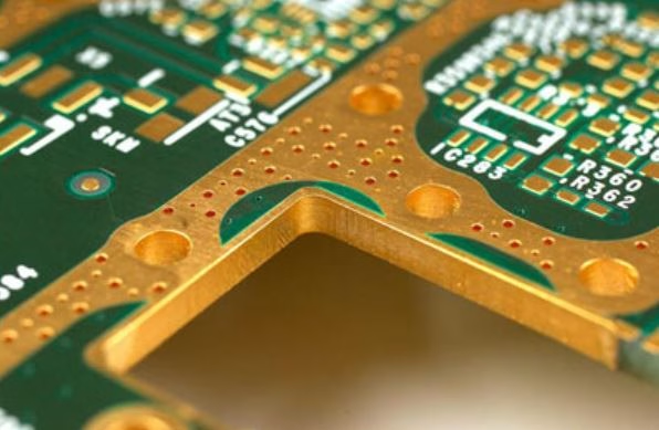
Enhance Signal & Durability with PCB Edge Plating
PCB edge plating or edge metallization, involves applying a conductive metal layer to the board's edges for improved electrical and mechanical performance.
Get Your PCB Quote!

Table of Contents
- 1¿Qué exactamente? i¿Recubrimiento de bordes de PCB?
- 2¿Por qué es crucial el enchapado de bordes?
- 3. Aplicaciones comunes de PCB Revestimiento de borde
- 4Consideraciones de diseño para un enchapado de bordes impecable
- 5El proceso de fabricación of Recubrimiento de borde de PCB
- 6. Superando desafíos en PCB Revestimiento de borde
- 7Recubrimiento de bordes de PCB Preguntas Frecuentess
- 8. Resumen
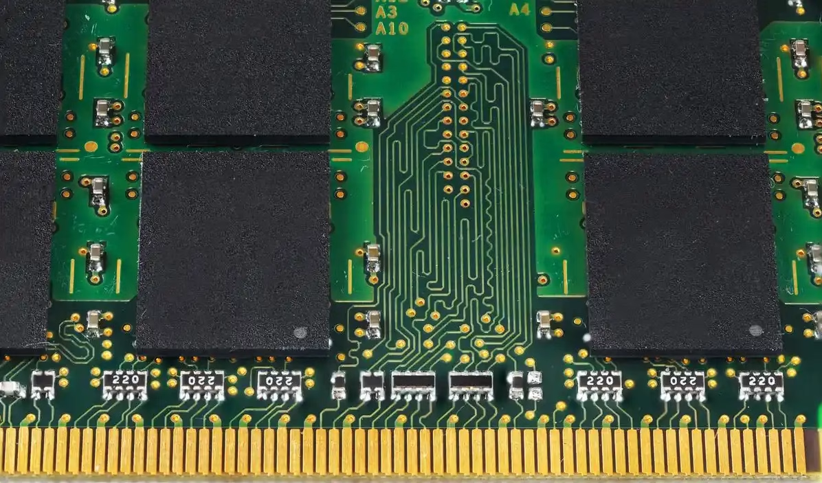
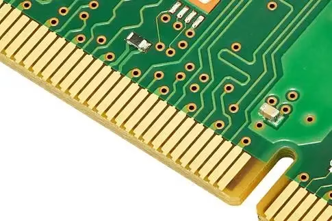
In the rapidly evolving world of electronics, where devices are constantly shrinking while demanding increased functionality and reliability, innovative manufacturing techniques are paramount. Among these, PCB edge plating has emerged as a critical process. Also known as edge metallization or castellated holes, this specialized technique involves applying a conductive metal coating, typically copper, to the perimeter edges of a PCB substrate.
This process is far more than a cosmetic finish; it creates reliable electrical connections between different layers of the board, or between the PCB and external components or enclosures. For engineers and hobbyists alike, understanding the intricacies of PCB edge plating is essential for designing high-performance, durable, and electromagnetically compatible electronic devices. This comprehensive guide will delve into the what, why, and how of PCB edge plating, providing a solid foundation for its effective implementation.
1. What Exactly is PCB Edge Plating?
PCB edge plating is a manufacturing technique where a continuous layer of conductive metal, most commonly copper, is deposited along one or more edges of a printed circuit board. This conductive layer extends from the top surface to the bottom surface, effectively connecting the outer layers and sometimes internal layers to the board’s periphery. The concept is straightforward: to create a robust, uninterrupted electrical path along the edge.
You might encounter several terms used interchangeably to describe this process, including side plating, border plating, or edge metallization. When the plating is applied to half-cut or perforated holes along the edge, these are specifically referred to as castellated holes. Regardless of the nomenclature, the core principle remains the same: to enhance the board’s functionality and performance through edge conductivity.
For beginners, it’s helpful to visualize it as wrapping a conductive skin around the board’s edge. This ” skin” can then serve multiple purposes, from shielding sensitive signals to creating strong mechanical and electrical interfaces with other parts of an electronic assembly.
2. Why is Edge Plating Crucial?
The implementation of PCB edge plating offers a multitude of advantages that significantly improve the performance, reliability, and longevity of printed circuit boards. Its importance stems from addressing critical challenges in modern electronics, particularly in areas like signal integrity, thermal management, and mechanical robustness. Here are the primary benefits:
1) Enhanced Electrical Connectivity
One of the foremost reasons for edge plating is to create superior electrical connections. It provides a continuous conductive path that can connect internal ground planes to external enclosures, improving grounding. It can also link various layers of a multilayer board directly to the edge, facilitating connections to other modules or components through direct soldering or pressure contacts.
2) Superior EMI/RFI Shielding
Electromagnetic Interference (EMI) and Radio Frequency Interference (RFI) are pervasive issues in electronic designs. Edge plating provides an effective conductive barrier around the perimeter of the PCB. This barrier acts as a Faraday cage, containing electromagnetic radiation generated by the components on the board, and conversely, protecting the internal circuitry from external interference. This is particularly crucial for sensitive circuits, high-frequency applications, and RF modules where signal integrity is paramount.
3) Improved Grounding and Thermal Management
A robust ground connection is vital for circuit stability and noise reduction. Edge plating allows for a direct and low-impedance connection to the system ground, which is often tied to a metal enclosure. This not only enhances grounding but also aids in thermal management. A larger conductive area at the edge can help dissipate heat away from critical components, improving overall system reliability and extending component lifespan.
4) Mechanical Reinforcement
Beyond electrical functions, edge plating significantly improves the mechanical integrity of the PCB. The deposited metal layer acts as a reinforcement, particularly on the edges that might be subjected to stress during assembly, handling, or in the final application. This mechanical reinforcement helps prevent delamination and adds to the overall durability of the board, making it more resilient in harsh environments or high-vibration applications.
5) Advanced Module Integration (Castellated Holes)
Castellated holes are a specific form of edge plating where half-cut, plated through-holes are present along the board’s edge. These features are invaluable for module-on-module designs, allowing smaller PCB boards (modules) to be easily and reliably soldered onto larger baseboards. The castellated holes provide pre-tinned, highly reliable solder points, simplifying assembly and enabling compact, modular designs common in IoT devices, sensors, and other miniaturized electronics. This technique facilitates easier inspection of solder joints, enhancing manufacturing efficiency and reliability.
| Benefit Category | Key Advantage | Impact on PCB Performance |
| Electrical | Continuous conductivity | Stable signals, lower impedance, improved grounding |
| EMI /RFI | Shielding barrier | Reduced noise, compliance with EMC standards |
| Thermal | Heat dissipation | Extended component life, improved reliability |
| Mechanical | Edge reinforcement | Increased durability, reduced delamination risk |
| Integration | Castellated holes | Simplified module assembly, compact design |
3. Common Applications of PCB Edge Plating
Given its diverse benefits, PCB edge plating finds applications across a wide spectrum of industries and electronic products. Its ability to enhance electrical performance, provide shielding, and offer mechanical robustness makes it indispensable for many modern designs.
1) RF and Microwave Circuits: For high-frequency applications, signal integrity and EMI control are paramount. Edge plating provides effective shielding to prevent signal leakage and external interference, making it critical for components like antennas, transceivers, and radar systems.
2) Module Integration: As mentioned, castellated holes are widely used for creating smaller, independent modules (e.g., Wi-Fi modules, Bluetooth modules, microcontrollers) that can be easily surface-mounted onto a larger main PCB. This modular approach simplifies manufacturing, testing, and replacement.
3) Wearable Devices and Miniaturized Electronics: In devices where space is at a premium, edge plating allows for direct connections to enclosures or other components without requiring additional connectors, contributing to smaller form factors.
4) Automotive and Aerospace Electronics: These sectors demand extreme reliability and durability. Edge plating enhances mechanical strength and provides robust electrical connections that can withstand vibrations, temperature fluctuations, and harsh operating conditions.
5) Power Electronics: For boards handling high currents or power, improved grounding and thermal dissipation capabilities offered by edge plating can prevent overheating and ensure stable operation.
6) LED Substrates: In certain LED applications, edge plating can be used for thermal management or direct electrical contact.
4. Design Considerations for Flawless Edge Plating
Achieving successful PCB edge plating requires careful consideration during the design phase. Adhering to specific guidelines ensures the plating process is effective and the final product meets desired performance and reliability standards.
1) Material Selection: While copper is the primary metal for edge plating due to its excellent conductivity and adhesion, the final surface finish (e.g., ENIG, HASL, Immersion Tin ) for the pads connecting to the edge plating must also be considered for soldering and environmental protection.
2) Plating Thickness and Tolerances: The desired thickness of the conductive metal layer must be specified. Manufacturers typically work within certain tolerances. Thicker plating offers better conductivity and mechanical strength but can also impact cost and process complexity.
3) Edge Clearance and Corner Rounding: For plating to adhere properly, there must be sufficient copper features (pads, traces, planes) extending to the edge of the board. Sharp corners should generally be avoided; rounded corners facilitate better plating adhesion and reduce stress concentrations. A minimum clearance from internal features to the plated edge might be required by the manufacturer.
4) Drilling and Routing: The edges designated for plating must be precisely routed. For castellated holes, the half-cut holes need to be drilled with high accuracy. The routing path must expose the copper layers to be plated.
5) Non-Plated Areas: Designers must clearly define which edges require plating and which do not. This is communicated through Gerber files, often using specific layers or attributes.
6) IPC Standards: Adhering to relevant IPC standards (e.g., IPC-6012, IPC-A-600) for PCB fabrication provides a framework for quality and reliability in edge-plated boards.
5. The Manufacturing Process of PCB Edge Plating
The manufacturing process for PCB edge plating is a specialized sequence that requires precision and controlled environments. While specific details may vary between fabricators, the core steps remain consistent:
1) Board Preparation: The PCB panel is prepared, including lamination of copper layers and dielectric materials.
2) Drilling: All necessary holes, including vias and holes for castellated features, are precisely drilled. For edge plating, the outer profile of the board is routed or scored after initial plating steps, or in some cases, partially routed before plating.
3) Cleaning and Desmearing: The drilled holes and routed edges are meticulously cleaned to remove debris and resin smearing (desmearing), ensuring optimal adhesion for the subsequent plating layers.
4) Electroless Copper Deposition: A thin, non-electrolytic layer of copper is chemically deposited onto all exposed surfaces, including the walls of the holes and the routed edges. This provides an initial conductive base.
5) Imaging and Pattern Plating: The board is then coated with a photoresist. UV light exposes the design pattern, leaving only the desired copper features (traces, pads, edge plating areas) exposed. Electroplating then adds a thicker layer of copper onto these exposed conductive areas, followed by a tin or nickel layer for protection.
6) Strip, Etch, and Final Finish: The photoresist is stripped away, and the exposed copper areas (not protected by the tin/nickel layer) are etched to form the final circuitry. Finally, a surface finish (e.g., ENIG, HASL ) is applied to all exposed copper pads, including those along the plated edge, to ensure solderability and protect against oxidation.
7) Edge Routing/Milling: If the edge plating is for the overall board contour or castellated holes, the final precise routing or milling of the board’s outline is performed. For castellated holes, this involves milling through the plated holes to create the characteristic half-cylindrical features.
6. Overcoming Challenges in PCB Edge Plating
While highly beneficial, PCB edge plating presents its own set of manufacturing challenges that must be addressed to ensure quality and reliability. Common issues include:
1) Uneven Plating: Achieving a uniform thickness of metal along the entire edge can be difficult, especially on complex geometries or sharp corners. This can lead to areas of insufficient conductivity or mechanical weakness.
2) Voids and Delamination: Poor adhesion of the plating to the substrate or internal copper layers can result in voids (unplated areas) or delamination (separation of the plated layer), compromising electrical integrity and mechanical strength .
3) Contamination: Residues from drilling, cleaning, or handling can prevent proper metal adhesion, leading to defects.
4) Etching Issues: Over -etching or under-etching can affect the integrity of the plated edge and the surrounding copper features.
To overcome these challenges, manufacturers employ stringent quality control measures, including precise drilling, thorough cleaning processes, optimized plating bath chemistries, and advanced routing techniques. Designers must also ensure their designs adhere to manufacturing capabilities and provide adequate allowances for plating processes to mitigate these risks effectively.
7. PCB Edge Plating FAQs
The primary metal used is copper due to its excellent electrical conductivity. Often, a subsequent layer of nickel and /or gold (e.g., Electroless Nickel Immersion Gold – ENIG) is applied as a surface finish for solderability and corrosion protection, especially for castellated holes.
Yes, edge plating is a specialized process that adds complexity to manufacturing, thus increasing the overall cost of the PCB compared to a standard board without this feature. However, the benefits in performance, reliability, and potential system-level cost savings often outweigh this added expense.
Most PCB boards can be designed with edge plating, but specific design rules and manufacturer capabilities apply. Considerations like minimum board thickness, copper feature placement near the edge, and corner radii are important. It’s best to consult with your PCB fabricator early in the design phase.
Edge plating refers to plating the entire or partial perimeter of a board. Castellated holes are a specific type of edge plating where half-cut, plated through-holes are created along the board’s edge. Castellated holes are specifically designed for module integration via surface mounting.
8. Summary
PCB edge plating is an indispensable technique in modern electronics manufacturing, offering a wealth of advantages that go beyond simple connectivity. From providing robust EMI shielding and enhanced grounding to offering crucial mechanical reinforcement and enabling advanced module integration via castellated holes, its role in improving PCB performance and reliability is profound. Understanding the technical specifications, careful design considerations, and the precise manufacturing process involved is critical for electrical engineers and designers seeking to optimize their printed circuit board layouts. By leveraging the power of edge metallization , manufacturers can produce more durable, efficient, and electromagnetically compatible electronic devices that meet the rigorous demands of today’s technology landscape.

Get Quote Free