
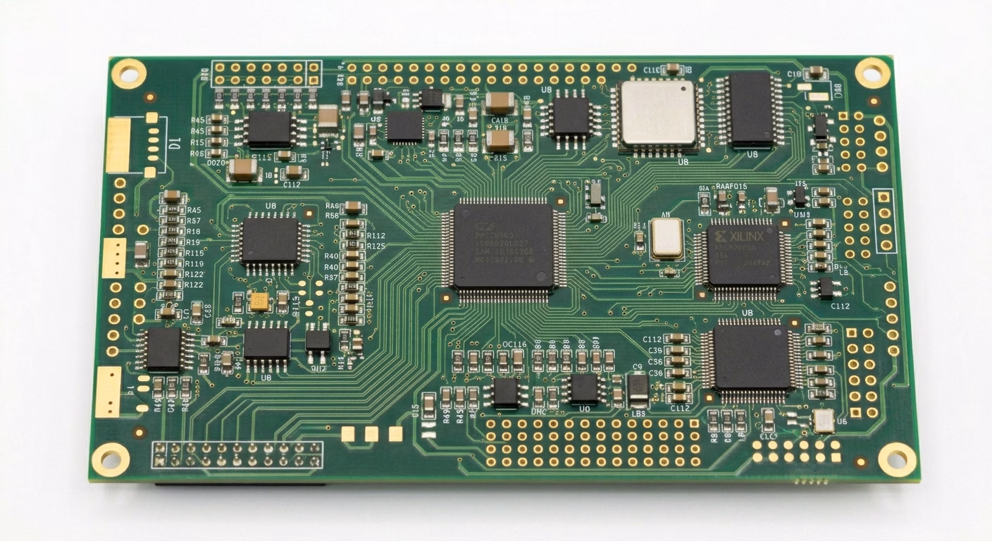
What is a Multilayer PCB?
A multilayer PCB is a printed circuit board (PCB) that consists of three or more layers of conductive material. These layers are separated by insulating materials and are interconnected through vias, including blind vias, buried vias, or through-hole vias. The complexity and high density of multilayer PCBs allow for higher circuit integration within a limited space.

Multilayer PCB Suppliers, China
As a leading multilayer PCB supplier in China, we offer a wide range of products tailored to various industries. Many suppliers like PCBAndAssembly focus on high-quality materials and advanced manufacturing techniques.
PCBAndAssembly stands out among these suppliers because we prioritize quality and timely delivery, always ensuring customer satisfaction. Moreover, our extensive experience in multilayer PCB production sets us apart from competitors.
PCBAndAssembly is a PCB and PCB assembly manufacturer with over 14 years of experience in producing multilayer PCBs. We offer one-stop services ranging from PCBs to PCBA, using a full range of raw materials and adhering to IPC Class 3, RoHS, and ISO9001:2008 standards. Serving customers worldwide, our professional team is ready to assist with even the most complex requirements.
Our Multilayer PCB Manufacturer Capabilities
Advantages of Multilayer PCBs
High Density
Multilayer PCBs allow for the stacking of multiple layers of circuits within a limited space, enabling the integration of more electronic components and connections within the same size.This high-density design is particularly suitable for modern electronic devices that require complex circuits, such as smartphones and laptops. High-density designs not only save space but also enhance the overall performance of the circuits.
Miniaturization
By compressing multiple layers into one PCB, the overall size of the circuit board can be significantly reduced.This miniaturization allows devices to be designed more compactly and portably, which is especially important for consumer electronics that require sleek designs, such as tablets and smartwatches.
High Performance
The multilayer structure can effectively reduce electromagnetic interference and signal loss, thereby improving the electrical performance of the circuit.Independent power and ground layers provide better power distribution and signal integrity, ensuring stable transmission of high-speed signals, which is crucial for high-speed data communication devices such as servers and routers.
Design Flexibility
Multilayer PCBs offer more design options, allowing for the easy implementation of complex circuit layouts.Designers can increase the complexity and functionality of circuits by adding more layers, enabling the integration of multiple subsystems on a single board. This is particularly important in military and aerospace applications.
Disadvantages of Multilayer PCBs
High Manufacturing Cost
The manufacturing process of multilayer PCBs is complex, involving more materials and steps.Producing multilayer PCBs requires high-precision equipment and process control, such as layer alignment and multiple laminations, which significantly increases production costs. Additionally, the use of high-quality raw materials (e.g., high Tg substrates) further drives up costs.
Complex Design
Designing multilayer PCBs requires a higher level of expertise and technology.Designing multilayer PCBs involves considering multiple factors, such as signal integrity, power management, and thermal management, which demand more skills from designers and require more design and testing time.
Difficult to Repair
Once a multilayer PCB is damaged, it is very difficult to repair.The multilayer structure complicates fault localization and repair, especially when internal layers are involved. Repairing multilayer PCBs usually requires specialized equipment and techniques, potentially leading to high repair costs.
Long Production Cycle
The manufacturing and testing process for multilayer PCBs is more time-consuming than for single-layer or double-layer PCBs.Multilayer PCBs require multiple laminations, drilling, and plating, which take more time and effort. Additionally, complex electrical testing and quality control processes extend the production cycle further.

Why Are Multilayer PCBs Needed?
Multilayer PCBs are crucial in modern electronic devices because they enable high-density and high-performance circuit designs within a limited space. As electronic products become more complex, multilayer PCBs offer more design flexibility and higher electrical performance, meeting the demands for high-speed signal transmission and low noise.
How to Manufacture Multilayer PCBs?
The manufacturing process of multilayer PCBs includes the following main steps:
- Material Preparation: Select appropriate substrate materials and copper foils.
- Lamination: Laminate multiple single-layer PCBs together using insulating materials and heat pressure.
- Drilling: Use laser or mechanical drilling techniques to create through holes and blind vias.
- Plating and Etching: After drilling, plate the holes to interconnect the layers, and then use etching techniques to create circuit patterns.
- Layer Alignment: Ensure precise alignment between layers to avoid shorts or opens.
- Surface Treatment: Apply protective coatings or pad surface treatments to enhance reliability.
- Testing: Conduct electrical and functional tests to ensure the PCB meets design specifications.
Why Choose Multilayer PCB Manufacturers in China?
Multilayer PCB manufacturers in China, like PCBAndAssembly, offer a wide range of materials, sophisticated technology, tailor-made solutions, and a secure supply chain. At PCBAndAssembly, we provide innovative solutions at competitive prices, and we have the capacity for large-scale production.
- Manufacturers offer a variety of materials for specific applications.
- You can choose from standard and high-frequency materials.
- Many manufacturers utilize state-of-the-art equipment.
- This technology ensures high precision and quality in production.
- Manufacturers can tailor designs to meet unique requirements.
- Customization helps optimize performance for specific applications.
- China has a robust supply chain for electronic components.
- This network supports timely procurement and assembly services.
Multilayer PCB Layout Design
The layout design of multilayer PCBs needs to consider the following aspects:
- Power and Ground Layers: Use separate power and ground layers to reduce noise and signal interference.
- Signal Integrity: Ensure signal paths are as short and direct as possible to reduce signal reflection and interference.
- Thermal Management: Design adequate thermal channels and vias for efficient heat dissipation.
- Trace Spacing: Design appropriate trace spacing according to electrical requirements to avoid shorts and signal crosstalk.
- Via Design: Optimize the position and number of vias to reduce electrical loss and manufacturing complexity.

Considerations for Manufacturing Multilayer PCBs
- Material Selection: Ensure the appropriate substrate and insulating materials are chosen to meet electrical performance and thermal management requirements.
- Precision Control: Ensure the precision of drilling and layer alignment to avoid manufacturing defects.
- Cost Control: Optimize manufacturing processes and material usage to control costs.
- Quality Inspection: Implement strict quality inspection processes to ensure products meet design specifications.
Applications of Multilayer PCBs
- Communication Equipment: Mobile phones, routers, and switches.
- Computers and Storage Devices: Servers, motherboards, and hard drives.
- Medical Devices: MRI, CT scanners, and ECG machines.
- Consumer Electronics: Smartphones, tablets, and wearable devices.
- Automotive Electronics: Car navigation systems, ADAS, and electric vehicle control systems.
Multilayer PCB Fabrication | FAQs
How are multilayer PCBs made?
Multilayer PCBs are made by laminating alternating layers of conductive copper and insulating substrate under controlled heat and pressure. Inner layers are imaged and etched to form circuit patterns, then bonded using prepregs and copper foils.
Drilled holes create vias and are plated to establish electrical connections between layers. Outer layers are imaged, etched, coated with solder mask, and finished with surface treatments such as ENIG or HASL. Final inspection includes electrical testing, impedance control verification, and dimensional checks.
What are the benefits of multilayer PCBs?
Multilayer PCBs provide higher circuit density and compact layouts, allowing multiple routing layers within limited space. This reduces the overall footprint of electronic products and improves electrical performance by shortening signal paths and minimizing stray capacitance and crosstalk.
Compared to single-sided or double-sided boards, multilayer PCBs support complex applications that require high-speed signaling, improved power distribution, and mechanical strength.
What is the maximum recommended aspect ratio for vias in multilayer PCBs?
The maximum recommended aspect ratio for vias is 25:1. This ratio, which compares board thickness to via diameter, maintains reliable electrical connections and prevents plating defects such as voids or barrel cracking during manufacturing.
What are the design considerations for multilayer PCBs?
Stackup design should separate signal layers with continuous ground or power planes to reduce EMI and crosstalk. Controlled impedance routing must account for dielectric constants, trace widths, and layer spacing to maintain signal integrity, especially in high-speed designs.
Via choices—blind, buried, and copper-filled—must balance routing density with mechanical strength. Using high TG FR4 or Rogers laminates improves heat dissipation in dense layouts. Designers must also address manufacturing tolerances, maintain via aspect ratios at or below 25:1, and control panel warpage for reliable performance.