Reliable Medical PCB Assembly for Life-Saving Electronic Devices
Medical PCB assembly delivers the safety and reliability standards that modern medical devices demand, with certified quality management and full regulatory compliance. We provide medical PCBA solutions for implantable, diagnostic, and monitoring devices with fast turnaround times and flexible order quantities.
14+
Years Experience
98.15%
On-Time Delivery
96%
customer satisfaction rate
99%
Quality Pass Rate
Importance of Medical PCBs
Medical PCBs play a critical role in the healthcare industry by ensuring accurate and reliable operation of medical devices. These specially designed PCBs can withstand the demanding requirements of medical environments, enabling precise signal processing, compact layouts, and rugged environmental resilience. Medical PCBs help provide high-quality medical services by supporting crucial tasks like patient monitoring, diagnostic imaging, and more.
The high reliability and regulatory compliance of medical PCBs make them indispensable components in medical devices, elevating patient care and advancing medical technology. Benefiting from optimized compact layouts, medical PCBs enable integration of complex circuitry to optimize medical device performance. Their stable and dependable performance improves medical workflows, enhances diagnostic accuracy, and benefits patients. In the medical field, the importance of medical PCBs is indispensable.
Our Medical PCB Assembly Capabilities
Why Choose PCBAndAssembly for Your Medical PCB Assembly?
What are Medical PCBs?
Medical PCBs are printed circuit boards used in electronic medical devices where failure poses patient risk. These assemblies meet IPC Class 3 reliability standards and are built using high-Tg, low-loss laminates such as polyimide, Teflon, and RO3003 for thermal and electrical stability.
PCBAndAssembly fabricates medical PCBs with 1.8 mil trace widths, up to 28 oz copper, and dielectric control to ±10%. All medical PCBA builds include AOI, solderability testing, and ionic cleanliness control below 1.56 µg/cm² NaCl equivalent.
Our workflows are structured to align with FDA 21 CFR Part 820, which governs quality system regulation (QSR) for medical device manufacturing in the United States, and the standards maintained by the IPC (Association Connecting Electronics Industries), which defines global benchmarks for PCB design, performance, and assembly.
Applications range from wearable monitors to HDI neuromodulators, each requiring ISO 13485-compliant traceability, reflow documentation, and component lot tracking.
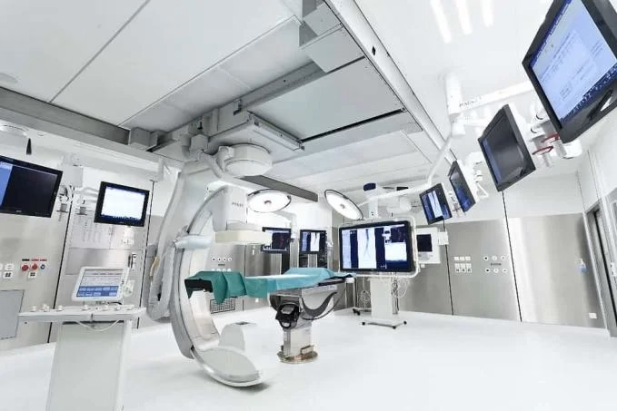
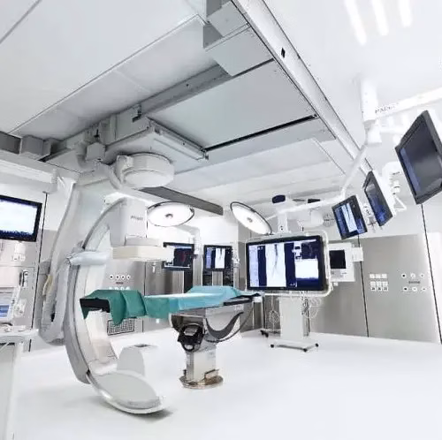
Applications of PCBs in Medical Devices
PCBs have extensive applications in medical fields including medical imaging equipment, vital signs monitoring devices, medical diagnostic devices, implantable medical devices, surgical instruments, portable medical devices, and more.
PCBs play an essential role in these devices, enabling precise signal processing, data transmission, control, and feedback mechanisms, ensuring reliable and accurate operation for medical diagnostics, monitoring, and treatment, ultimately contributing to enhanced patient care and healthcare outcomes.Some typical applications of these medical PCBs include:
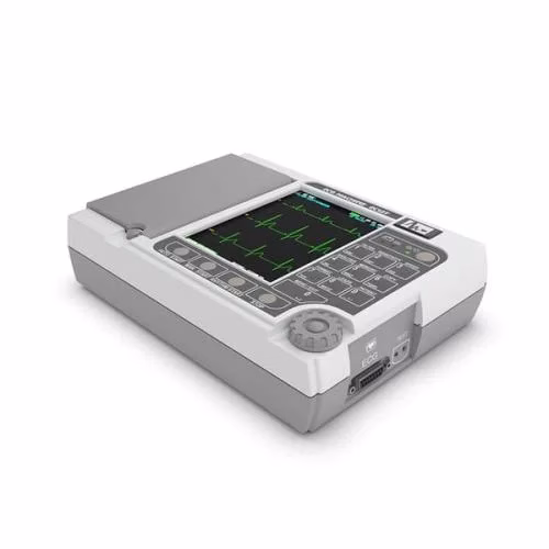
ECG machines
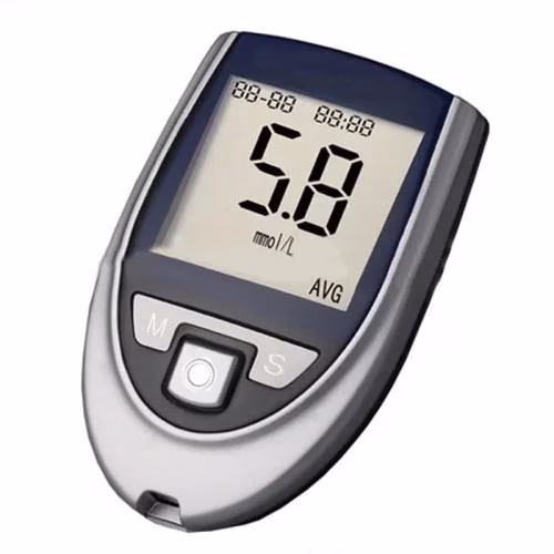
Blood glucose monitors
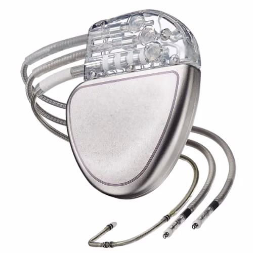
Pacemakers and defibrillators
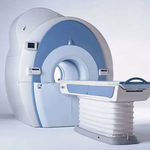
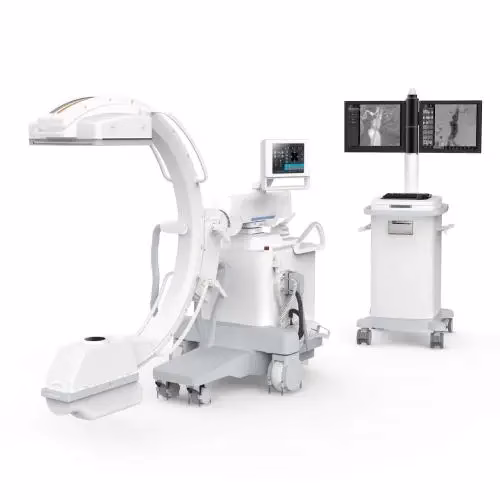
X-ray and MRI equipment
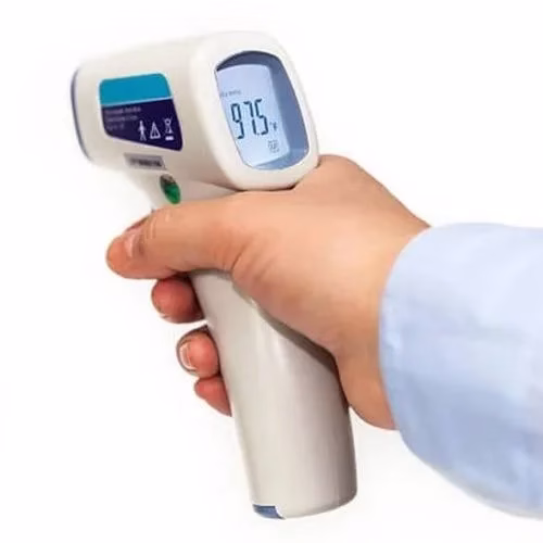
Thermometers and medical sensors
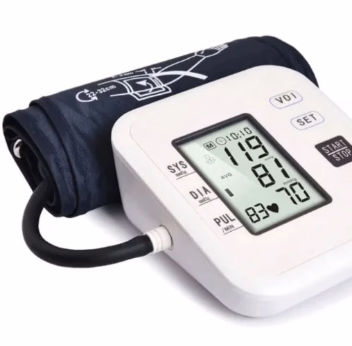
Blood pressure monitors
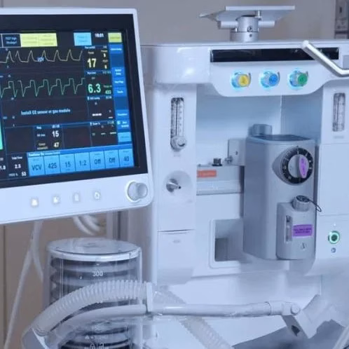
Ventilators and oxygen supply equipment

robotic-assisted surgery devices
Medical diagnostic instruments
Medical image processing and display equipment
Common Applications of Medical PCBs
Design for Manufacturing Considerations for Medical PCBs
PCB standards for the medical industry
In the medical industry, PCB (Printed Circuit Board) standards play a crucial role in ensuring the safety, reliability, and performance of PCBs used in medical devices. These standards define the specific requirements and guidelines that PCBs must meet to be suitable for medical applications. Some of the prominent PCB standards for the medical industry include:
- IPC-A-600: This standard, published by the Association Connecting Electronics Industries (IPC), outlines the acceptability of PCBs regarding surface conditions, hole quality, conductive patterns, and other critical aspects.
- IPC-A-610: Also published by IPC, this standard provides criteria for the acceptance of PCB assemblies, ensuring that they meet the necessary workmanship standards for medical devices.
- ISO 13485: Although primarily focused on quality management systems, ISO 13485 also covers aspects related to PCB design, manufacturing, and control for medical devices.
- IEC 60601-1: As mentioned earlier, this standard applies to medical electrical equipment and systems, specifying safety and performance requirements that PCBs in medical devices must adhere to.
- IEC 61010-1: This standard specifically addresses safety requirements for electrical equipment for measurement, control, and laboratory use, which includes many medical devices with PCBs.
- UL 60601-1: UL certification ensures that the PCBs and electrical components used in medical devices meet safety and performance standards as required by UL.
- RoHS (Restriction of Hazardous Substances) Directive: While not directly a PCB standard, RoHS compliance restricts the use of hazardous substances in PCBs, making them safer for medical device applications.
- IEC 62368-1: This standard applies to electrical and electronic equipment within specific voltage ranges and ensures safety requirements for PCBs used in medical devices.
- J-STD-001: This standard, also published by IPC, defines the requirements for the soldering of electrical and electronic assemblies, including medical PCBs.
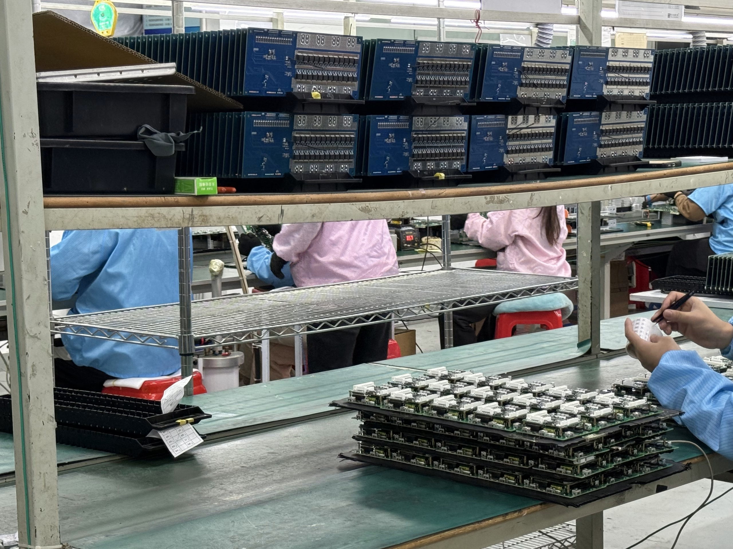
PCB Factory Gallery