Panel Creation
For cost-saving or technical reasons (such as improved assembly), multiple circuit boards may be combined to form a “panel”. This panel is then produced just as a single large circuit board. A separation of the panel does not occur!
PCBAndAssembly, as the most professional manufacturer in this field for more than a decade. We can make the boards according to your panel design. Also, we can provide the service to help you panel the single board for free.
Please pay attention to fiducial marks or location holes during the design process.
Location holes are non-plated-through holes (Npth), which allow an accurate positioning of the printed circuit board for processing. The placement of the location holes is based on the requirements of the machine used, usually asymmetrically in order to avoid a rotated position. The custom-fit catching of the holding pins allows a very low tolerance for further processing.
In printed circuit board production, location holes help with stack processing, e.g. drilling
or milling of a whole stack of printed circuit boards.
What is the PCB panel?
That means we help you connect the single boards(same or different are both OK) on one big panel by different route process, then it will be easy for you to break them into single PCB. For the routing process, it has three types: V-scoring, Tab route, and stamp holes.
V-scoring
Panel with V-Cut/V-Scoring/V-Groove
For V-scoring panelization, space between boards can be 0mm or 2mm.

V-scring has to be continuous and can not be stopped in panel, if you have many different boards like following image to be panelized, we suggest add tab routes between boards instead of V-scoring.
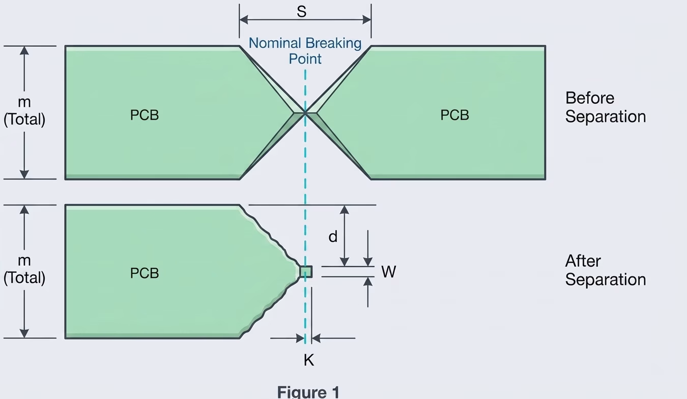
V-scoring is the most popular way in the PCB panel. V-scoring is the v-shape line to connect boards for convenience separation. We also require the v-scoring boards, please observe the following rules:
The gap between the individual circuit boards in the layout is 0mm based on the minimum spacing between copper pattern (trace/pad/copper ground) and V-cut line is 0.4mm.
Scoring lines must be straight; horizontal and vertical lines are possible, so the board’s frame must be regular, and the size of boards must be over 45mm*60mm.
For stability, We recommend using V-scoring only for board thicknesses greater than 0.6mm.
More information about V-scoring,please check PCB V-Scoring.
Tab route and stamp holes
For tab route and stamp holes, it can be used in the irregular boards. However, For the tab route, the space between boards should be 1.6mm.
For panel with tab routes, 1.6mm space is needed between boards. There are 2 kinds of tab routes be used for panel. One is tab route with breaking holes(stamp holes) and the other one is tab route with tab(no holes).

Panel with Tab Route
Tab route with breaking holes(stamp holes)
For tab route with breaking holes diameter should be ≥0.45mm, regular diameter is 0.55mm-0.6mm. Holes space has to be ≥0.35mm, usually we will add 5-6 holes to each tab.

Tab route with breaking holes
Tab route with tab
Tab route with tab,tab width has to be at least 2mm.

Tab route with tab
The Advantages of PCB Panel
- Mass production: If you need to build a large number of PCBs, panelization will save you time and money.
- Product Safety: Panelization protects the PCB from shock and vibration during assembly.
- Speed and efficiency: From paste printing to component assembly, soldering, and even testing, as part of a large array, processing multiple boards at once is faster and more efficient.