
How to Make PCB? Detailed PCB Production Process!
Get Your PCB Quote!
Table of Contents

With society and electronic technology rapidly progressing, Printed Circuit Board manufacturing techniques continue to evolve at an alarming rate. Here, Pcbandassembly will give a comprehensive introduction to PCB processing technology, including its basic concepts, main process flows, and technological developments.
1. Overview of PCB Processing Technology
PCB processing technology is the process of converting circuit design graphics into actual circuit boards. It involves multiple process steps, including circuit board design, material preparation, pattern transfer, etching, drilling, surface treatment, etc. These steps together ensure the high precision, high reliability and high performance of PCB.
2. Main Process Flow of PCB Processing
What are the process flows of PCB board making? From watches and headphones to military and aerospace, PCB circuit boards are present in almost all electronic products. Although widely used, most people don’t know how PCB is produced. Next, let us take a detailed look at the production process of PCB!
In the eleven steps summarized below, each process requires multiple techniques for fine processing and production. It should be noted here that the PCB processing and production processes are different for boards with different structures and materials. The following is a detailed discussion taking the production and processing technology of multi-layer PCB as an example.
1) Design Stage
Circuit design: When creating circuit diagrams and PCB layouts, designers rely on electronic design automation (EDA) tools to produce circuit diagrams and PCB layouts, identify circuit functions, arrange components on PCB boards and determine wire paths etc.
File preparation: Convert designed PCB layout files to production-oriented formats like Extended Gerber RS-274X or Gerber X2, then check that they meet production process requirements.
2) Raw material Preparation
Substrate material: Select substrate material that meets the design requirements, such as FR-4, etc.
Copper foil: Prepare copper foil for making circuit conductors.
Solder mask ink: Used to coat the surface of the PCB to protect areas that do not require soldering and prevent corrosion.
Silk screen ink: Used to print marks, text or patterns.
3) Inner Layer Production
Mainly for the production of the inner layer circuit of the Printed Circuit Board.
Let us first understand a few concepts:
CUT: The process of cutting the original copper-clad board into boards that can be made on the production line is called CUT
UNIT: The unit pattern designed by the PCB design engineer is called UNIT
SET: Engineers often put multiple Units together to form a whole pattern, which is called SET. This can improve production efficiency and facilitate assembly production.
PANEL: When PCB manufacturers produce, they put multiple Sets together and add tool board edges to form a board called Panel. This can improve efficiency and facilitate processing and production.
Inner Dry Film: The process of transferring the inner layer circuit pattern completely to the PCB board is called inner layer dry film.
The so-called dry film is actually a photosensitive film attached to the copper surface. It is very special. When it encounters light, it will solidify on the surface of the board, thus forming a protective film.
In the specific use process, the dry film will cause many problems. If it is not solved well, it will affect the use effect and product quality. First, the dry film will have holes. After the holes are broken, the film temperature and pressure should be reduced to improve the drilling flash, so that the toughness of the dry film can be kept unchanged. Do not try to increase the film temperature and pressure to enhance its bonding strength, which will cause excessive evaporation of the solvent, making the dry film brittle and thin, and it is very easy to be punched through the hole during development. Secondly, during electroplating, the dry film will be infiltrated. The reason for the infiltration is that the exposure energy, film temperature, and film pressure are not appropriate. This is an important process for the combination of dry film and PCB board. Work can only start after debugging according to the corresponding process requirements and parameter standards.
When designing circuits, engineers need to consider a variety of safety factors, among which the minimum line width, spacing control, and wiring uniformity are particularly noteworthy. Because too small a spacing will cause film sandwiching, and the film cannot be completely removed, which will cause a circuit short circuit and affect the safety of the circuit board. If the line width is too narrow, it will affect the adhesion of the film, resulting in an open circuit. During the production process, engineers must keep a good grasp of the safety distance. Whether it is between lines, between lines and pads, between pads and pads, or between lines and copper surfaces, it is very important to leave enough safety distance.
Okay, after understanding several important concepts, let’s get into the topic. The following is the inner layer production process:
Panel Cutting: Cut the PCB substrate into production size.
Inner Layer Cleaning(Grinding PCB): First we need to solve the problem of PCB substrate surface cleanliness and surface roughness. Clean the PCB board and remove the pollutants of the surface. This will remove the oxides on the copper surface and allow the dry film to adhere better to the copper surface.
Jointing Dry-film: Stick the dry film to the surface of the PCB substrate to fully prepare for the image transfer in the subsequent steps.
Laser Direct Imaging (LDI) Exposure: The laminated substrate is exposed to ultraviolet light from an exposure device, thereby effectively transferring the image of the substrate to the dry film.
When the PCB board with dry film is exposed, there is an image on the innermost layer of the dry film because the dry film is composed of three layers of materials. The middle layer is the dry film, which plays a functional role, and the two outer layers are transparent films, which play a protective role. When laminating, the inner protective film is torn off by the machine. After exposure and before development, the outer protective film must be torn off.
Factors affecting the quality of exposure imaging: The quality of the exposed image is difficult to grasp, and many factors can affect it. In addition to the performance of dry film, the choice of light source, the control of exposure amount, the quality of the baseplate, etc. have a profound impact on the quality of exposure imaging.
Developing: The developer sodium carbonate is used to dissolve and wash away the unexposed dry/wet film to reveal the exposed part.
Etching: To obtain the circuit, use acidic copper chloride in order to dissolve and corrode the part of the copper surface that is exposed.
Peeling Film: Remove the dry film protecting the copper surface by using sodium hydroxide to peel it off. This will reveal the circuit pattern, and the inner layer board is now complete.
4) Inner Layer Inspection and Repair
Mainly for inspection and repair of the board circuits.
AOI (Automatic Optical Inspection): AOI can scan the PCB board and compare it with the recorded data to detect defects, such as depressions and gaps on the board image.
VRS (Visual Repair System): VRS receives the defective image and transmits the data to the VRS to be inspected and repaired by the relevant personnel.
Wire repair: Solder gold wires in gaps or depressions to connect the circuits and avoid problems such as electrical leakage.
5) Lamination
As the name implies, multiple inner-layer boards are pressed into one board.
Brown Oxidized: A uniform, well-bonded organic metal layer structure is generated on the surface of the copper layer through chemical treatment, which better enhances the bonding strength between the inner copper layer and the prep reg after board pressing. Browning can increase the bond between the board surface and the resin, as well the moisture of the copper surface.
Lay-up: Multiple inner-layer boards are laminated with PP (Pre-pregnant).
During actual operations, materials such as copper foil, bonding sheets (prep reg), inner layers, stainless steel, isolation boards, Kraft paper and outer layers of steel plates are stacked in accordance with.
For designers, symmetry is the most important factor in the lamination step. Because the board is still stressed after lamination because it is affected by temperature and pressure during the process. Therefore, if the two sides of a laminated board do not have the same stress, it will cause the board to bend towards one side. It can be seen how much influence symmetry has on the printed circuit boards.
If the copper distribution on the same plane is uneven, then the resin flow rate will vary at each point, so the thickness will differ between the places with copper and those with copper.
In order to avoid the above problems, designers must fully consider many factors when designing circuits, such as uniform distribution of copper, symmetrical stacking of boards, reasonable design and layout of blind and buried holes, etc.
Lamination: The board is pressed into a whole under high temperature and high pressure.
Drilling, Edging and Grinding: Punch, edging and grinding the laminated boards.
6) Drilling
Drill corresponding holes in the plate according to the diameter and size required by the customer. This will allow through holes to be made for the subsequent processing of plug ins. It can also assist the board to dissipate its heat.
Positioning holes: Drill positioning holes for alignment in subsequent processing.
Through holes: Drill through holes according to design requirements to connect wires or plug-ins on different layers.
7) Outer Layer Production
Plated Through Hole: A copper layer with good conductivity is formed on the inner wall of the drilled hole and the surface of the PCB. After the drilling step, the PCB board undergoes a reduction-oxidation reaction in the copper plating tank to form a layer of copper, thereby metalizing the hole. Copper is then deposited onto the surface the original insulating substratum to achieve an electrical connection between layers.
Electroplating: Electroplating involves coating PCB boards with layers of metal films such as nickel, copper or gold to increase conductivity while acting as protection measures.
Dry Film: The outer layer graphics are transferred to the PCB using the principle of photochemistry.
Etching: Remove the unnecessary copper foil to form the final PCB conductor pattern.
8) Solder Mask and Silk Screen
Solder Mask: Apply a layer of solder mask ink onto the PCB surface to create the required solder mask area. Solder ink (also referred to as green oil) plays an integral part of manufacturing printed circuit boards. This is done by applying solder ink or screen printing to apply solder on the surface. Through steps such as exposure and development, the pads and holes can be exposed, which are required for soldering. Other places are covered in solder to prevent short-circuits during welding. Text, trademarks, or part symbols, are required by screen printed and printed onto the surface.
Silk Screen Printing: Printing marks, text or patterns on the surface of the PCB.
9) Surface Treatment
In order to ensure good soldering performance or electrical performance, surface treatment is a must. In fact, bare copper itself has good soldering performance, but if it is exposed to the air for a long time, it will be oxidized by moisture and exist in the form of oxides, so the copper surface must be treated so that it can remain as original copper for a long time. The most common ones are the following five: hot air leveling (HAS), organic coating (DSP), chemical nickel/immersion gold (ENID), immersion silver and immersion tin.
10) Outline and Processing
Computer numerical control Routing: Chamfer the edges of the PCB to improve pliability and safety.
V-CUT: Cut a V-groove on the PCB to facilitate cutting the board into independent small boards.
Appearance processing: Chamfer the appearance of the PCB board according to customer requirements.
11) Testing and Quality Inspection
Flying Probe Tester: Conductivity test and insulation test to ensure correct circuit connection.
FQC (Final Quality Control): The PCB size, aperture, board thickness, marking, etc. are carefully checked to ensure that they meet customer requirements. Finally, qualified products are vacuum packed for better storage and transportation.
3. Development of PCB Processing Technology
In recent years, PCB processing technology has made significant progress. In today’s society, high precision, high density, and high reliability are increasingly becoming the goals of PCB processing technology. Generally speaking, the following four technologies will be increasingly valued and widely used:
Laser direct imaging technology (LDI): Imaging directly on the board by laser eliminates the step of graphic transfer and improves processing accuracy and efficiency.
Buried hole and blind hole technology: Hidden holes are made in multilayer boards, which reduces the volume and weight of the circuit board and improves the connection density and reliability.
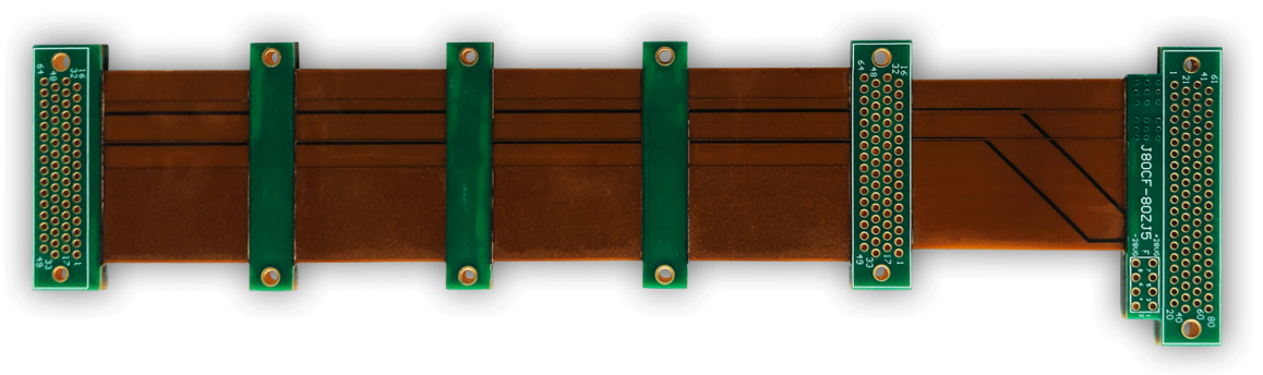
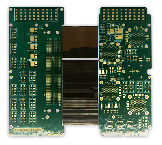
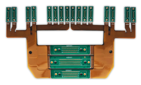
Flexible PCB technology: Flexible materials have been utilized in designing flexible circuit boards that offer improved bending and shock resistance, making them suitable for various complex environments.
Environmentally friendly materials and technologies: Utilizing eco-friendly materials and processes helps minimize pollution and environmental harm.
4. Summary
The process of circuit boards covers multiple links from preliminary preparation to finished product testing.
Of course, if you have any needs for printed circuit boards or electronic components or PCB assembly service or LED board assembly service, please feel free to contact us. At Pcbandassembly, we will wholeheartedly provide you with professional support and solutions.
The culture of our company and our process require a continuous cycle of communication during the design process. This includes listening, sharing our experience, and working collaboratively to meet the changing needs of the project. We are also always 100% committed.
Table of Contents

Get Your PCB Quote!


