
What Is PCB Design Called?
Get Your PCB Quote!

PCB design (Printed Circuit Board Design) refers to the design of circuit boards using electronic design automation software to design the layout and circuit connections of printed circuit boards.
The circuit board is a vital part of any electronic product. It can be used to connect electronic components and transmit signals via wires. PCB design is a process that transforms the circuit schematic into the circuit board layout and connections.
1.PCB Design: Key Points
The PCB design involves several basic concepts, and the following are several key points.
Overlay: The overlay is used to simplify the installation and maintenance, by displaying the logo and text code required on the upper and lower surface of the printed board, including the component mark, nominal value, shape, manufacturer’s mark and production date.
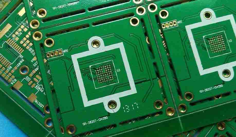
Pad: The most important and common concept in PCB layout is the plate (pad). When choosing the pad type for the element, shape, size and layout, vibration and heating conditions, and force directions should all be taken into consideration. There are a variety of sizes and shapes for welding pads. These include round, squares, star anise and round squares.
External Plane and Fill: The mesh filled area consists of a large area that has been processed into a grid, while the filled (Fill) is just copper foil. The first is used to fill large areas, such as those that are designated for shielding, segmentation, or large current power lines. The latter is mainly used to fill small areas, such as the line end and turning area.
Automatic wiring: A network connection to observe, like a rubber band. You can view the condition of the cross-connection of the network under “Show” after transferring components through the table. Then, adjust the components’ position to minimize the crossing to achieve the maximum automatic wiring rate.
PCB Proofing: PCB Proofing is the process of producing a printed circuit board in a small quantity before it goes into mass production. It is used by electronic engineers for circuit design and then sent to the factory after completion of PCB Layout for PCB testing. PCB proofing production is not limited by any specific quantity. Engineers call it PCB Proofing, before product design confirmation and test.
2. PCB Design: What to Consider?
The PCB design process takes into account the circuit performance requirements, reliability, EMC compatibility (electromagnetic compatibility), the manufacturing process and cost factors for PCB.
A good PCB design needs to consider the following aspects.
Plate, plate thickness, copper thickness, process, welding resistance / character color:
The R&D engineer should clearly write down the following: Plate, thickness of the plate, thickness of the copper, process, resistance to welding, color, etc.
Electromagnetic Compatibility:
If the PCB is not electromagnetically compatible, it may fail the 3C certification.
Power Supply Routing Strategy:
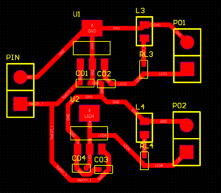
Any board must adhere to certain rules when it comes to the routing of power supplies. For each chip power pin, a 0.1uF capacitor must be placed to filter high-speed interference. The power supply and ground must be placed next to the line on a single-board to reduce the area of the return loop.
The Routing Strategy of Sensitive Signals:
Wrapping the ground is the best routing strategy for sensitive signals. This will allow the packet to take the shortest possible reflux path, and also eliminate interference from other adjacent signals.
Law of Minimum Signal Reflux Area:
In PCB design, every signal should be able to achieve the shortest possible reflux path to ground. The ground circuit can be made as short as possible on single and double surfaces. In order to make the ground for the multilayer plate it is required to place a large copper area in the layer adjacent. This adjacent layer is called the reference signal layer. This reference layer is used to calculate the size impedance when doing impedance design.
PCB Line Mode:
PCB lines cannot walk in a right angle, but can walk in a 45-degree Angle. The best circular arc is high-speed signal. Signal ultra-high speed 10 degree line. It is important to maintain a consistent thread width, or else it can cause an impedance discontinuity.
Routing Strategy:
It is best to route adjacent layers vertically. The first floor should be a horizontal line and adjacent layers should rout vertically. So, the adjacent layers’ signals will not interfere. If it is unavoidable then reduce the length of horizontal walking line segment. It is better to keep the distance below 1000mil.
The Number of Holes in the Power Line:
When connecting power lines with holes in multiple layers, it is important to consider the connectivity. The resistance of the hole can cause the voltage at the end to decrease if the current is high. We now add additional holes to the replacement connector.
Placement and Wiring of Capacitors:
The capacitor should be placed as close as possible to the chip pin. The wiring should also be as thick as possible and as short as is practical to achieve the best high-frequency filtering. It should not be connected with a long wire and then to ground.
Design of the Minimum Hole:
The cost is directly related to the size of the hole.
Line Width Spacing:
The larger the spacing between lines, the better.
Character Aspect:
The most important aspect of character design is the width and height of the words.
Weld Resistance:
Some copper skin or lines to show copper.
To ensure quality and performance, it is important to consider all of the above aspects when designing PCBs.
3. PCB Design Steps
Determine the circuit diagram: Circuit diagrams are required for PCB design. They facilitate subsequent layout and connections.
Schematic design: Draw the schematic design of the circuit. Include the connections between each component and the functions.

Establishment of PCB package library: Create a PCB library by packaging the components and creating the library.
PCB layout design: The schematic diagram is translated into the layout on the board and the connection relationships, including the size, shape, and position of each component, the layout of the wires, etc.
4. Basic Principles of PCB Design
Have a Reasonable Route Direction
These include input/output, AC/DC, strong/weak signal, high/low frequency, high/low pressure, etc. They should have a linear direction (or be separated), not to blend together, but to avoid mutual interference. It is best to press in a straight line. However, this is not always possible. The ring is the worst direction. The PCB requirements for DC, low voltage, small signal and low resistance can be reduced. Being “reasonable”, then, is relative.
Select a Good Docking Spot (Which Is Usually the Most Important)
It is important. I don’t know how many technicians and engineers have discussed it. The requirements for common points are generally: the forward amplifiers of multiple lines must converge, and then be connected to the main line, etc. It is not possible to complete the task due to the various restrictions. However, we must do our best. In practice, this problem is flexible, and everyone has their own solutions. If you can describe the specific circuit boards to understand, then it’s easy.
Arrangement of Filtering/Decoupling Capacitance in Power Supplies
In most schematics, only a few power supply decoupling/filtering capacitors are shown, but their connections are not specified. These capacitors are actually set up for components such as switching devices (gate-circuits) and other components that require filtering/decoupling. They should be placed as close as possible to these components, otherwise they won’t have any effect. When the filtering/decoupling power supply capacitors are arranged properly, the grounding point issue becomes less obvious.
Line Diameter and Thickness Is Appropriate
It is not acceptable to use right angles for turning if the condition of making a wide wire exists. High-frequency and high-voltage lines must be slick, without sharp chamfers. It is important to make the ground wire as wide as it can be. It’s also best to use as much copper as you can, as this will help with docking. The disc or wire pass holes are too small, or the pad size is not matched to the hole size. Both are not suitable for CNC drilling. The pad can be easily drilled into a “C”, and the weight will drill away the pad. The wire is thin and there is no copper in the large untiring area, so it is easy for corrosion to occur unevenly. When the untiring is corroded the thin wire will be likely to over-corrode, or appear broken or completely broken. Setting copper has a function other than to increase ground area or anti-interference.
Number of Solder Joints and Line Density
The smallest mistake in copper immersion can hide dangers. The design should reduce the number of via. It is difficult to weld together parallel lines that are too dense. The linear density of the lines should be based on the level of welding. It is impossible to manually weld because the distance between the solder joints is too short. The only way to improve the quality of welding is by reducing ergonomics. If you do not, there are hidden dangers. The quality and ergonomics should be taken into consideration when determining the minimum distance between the solder joints.
You can improve your design efficiency and quality by fully understanding and grasping the above PCB design considerations. Correction of existing errors during the production process can save time, money and materials.
5.Summary
The printed circuit board design is based on a circuit schematic diagram in order to meet the requirements of the circuit designer. The layout design is the main aspect of the design of printed circuit board. It involves a number of factors, including the layout of external connectors, the optimal placement of electronic components within the board, the layout of metal via and wires, electromagnetic shielding, and heat dissipation. A good layout design can reduce production costs, and improve circuit performance and heat dissipation. Computer-aided design is needed for complex layout designs.

Get Your PCB Quote!


