What are SMT Stencils? Different Types and Design Guidelines
The guide will take a deep dive into the world of SMT stencils, exploring their basic role, the different types available, the critical design considerations, and best practices to ensure precision and quality in your PCB assembly process.
Get Your PCB Quote!
Table of Contents
- 1. The Unsung Hero of SMT
- 2. What Exactly is an SMT Stencil?
- 3. Diverse World of SMT Stencil Types
- 4. The Science of SMT Stencil Design: Key Parameters
- 5. The SMT Stencil Printing Process: A Closer Look
- 6. Avoiding Pitfalls: Common Stencil-Related Defects
- 7. Selecting the Right SMT Stencil
- 8. SMT Stencil FAQs
- 9. Summary

1. The Unsung Hero of SMT
In the intricate world of electronics manufacturing, where miniaturization and high performance are paramount, the precision of Surface Mount Technology(SMT) is key. At the heart of achieving flawless circuit board functionality lies a seemingly simple yet absolutely critical tool: the SMT stencil. This thin, precisely manufactured sheet of metal dictates the accuracy of solder paste application, which, surprisingly, is often cited as the root cause of up to 60% of SMT assembly failures.
Without a well-designed and properly utilized SMT stencil, even the most advanced PCB assembly line can falter, leading to costly defects, rework, and production delays. This guide will take a deep dive into the world of SMT stencils, exploring their fundamental role, the different types available, the critical design considerations, and best practices to ensure precision and quality in your PCB assembly process.
Key Takeaways
- SMT stencils are vital for precise solder paste application, directly impacting PCB assembly.
- Up to 60% of SMT assembly failures can be traced back to stencil-related issues.
- Choose from framed, frameless, step, and nano-coated stencils based on production volume and complexity.
- Stencil thickness and aperture design(aspect and area ratios) are critical for optimal paste release and preventing defects.
- Regular under-stencil cleaning and proper alignment are essential for consistent stencil printing and defect prevention.
2. What Exactly is an SMT Stencil?
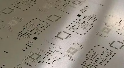
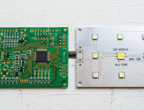
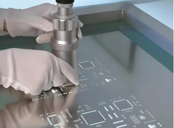
An SMT stencil, sometimes referred to simply as a PCB stencil, is a thin sheet of material, typically stainless steel or nickel, with laser-cut openings(apertures) that correspond precisely to the solder pads on a Printed Circuit Board(PCB). Its primary function is to facilitate the controlled deposition of solder paste onto these pads.
During the SMT process, the stencil is aligned over the bare PCB. A squeegee blade then sweeps solder paste across the stencil’s surface, forcing the paste through the apertures and onto the designated pads below. This precise application ensures that when components are placed and the board goes through reflow soldering, solid electrical connections are formed. The stencil’s accuracy directly impacts the quality of solder joints, making it an indispensable tool for reliable electronic product manufacturing.
3. Diverse World of SMT Stencil Types
Not all SMT stencils are created equal. Different applications, production volumes, and board complexities demand specific types of stencils. Understanding these variations is crucial for optimizing your assembly process.
3.1 Framed Stencils(Glue-in Stencils)
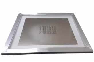
These are perhaps the most common type for high-volume production. A framed stencil consists of a laser-cut stencil foil permanently bonded to an aluminum frame using a mesh border. The mesh provides tension, ensuring a flat, taut surface that is critical for accurate solder paste deposition. They offer excellent durability and alignment stability, making them ideal for automated printing machines and continuous production runs. Their robustness makes them a reliable choice where consistent quality over many cycles is required.
3.2 Frameless Stencils(Re-usable Stencils)
Also known as foil stencils or reusable stencils, these are essentially just the laser-cut stencil foil without a permanent frame. They are designed to be used with a universal reusable stencil frame system that applies tension during the printing process. Frameless stencils are a cost-effective solution for prototyping, low-to-medium volume production, or for designs that may change frequently. They require less storage space and offer flexibility, though their setup time might be slightly longer compared to framed versions.
3.3 Step Stencils
Step stencils are specialized stencils where the thickness of the foil varies across different areas. This is achieved by either adding or removing material in specific regions of the stencil. The primary purpose of a step stencil is to control the volume of solder paste applied to different components on the same PCB. For example, larger components might require more solder paste(thicker stencil area), while very fine-pitch components need less(thinner stencil area). This allows for optimal solder joint formation across a board with mixed component types and sizes.
3.4 Electroformed Stencils
These stencils are created through an electrodeposition process, where nickel is built up on a master mandrel. Electroformed stencils are known for their extremely smooth aperture walls and trapezoidal openings, which significantly improve solder paste release, especially for ultra-fine pitch components and micro-BGAs. This smoother release reduces bridging and improves overall print quality, leading to fewer defects.
3.5 Nano-Coated Stencils
Regardless of the stencil type (framed, frameless, electroformed), a nano-coating can be applied to the stencil surface. This hydrophobic, non-stick coating reduces friction and improves solder paste release from the apertures. Benefits include fewer clogged apertures, reduced under-stencil cleaning frequency, and improved print consistency, especially for challenging fine-pitch applications. It enhances the efficiency and reliability of the printing process.
4. The Science of SMT Stencil Design: Key Parameters
The performance of an SMT stencil is heavily influenced by its design parameters. Precision in these aspects is paramount to prevent common printing defects.
4.1 Stencil Thickness
The thickness of the stencil directly controls the volume of solder paste deposited. A thicker stencil deposits more paste, while a thinner one deposits less. The challenge lies in balancing the requirements of different components on the same board. Too much paste can lead to bridging, while too little can result in insufficient solder or opens.
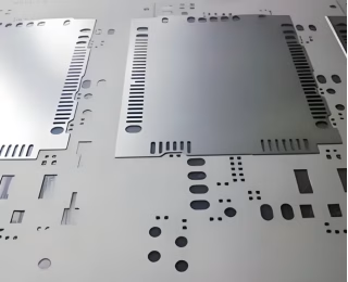
4.2 Aperture Design
The shape and size of the apertures are critical for proper solder paste release Key considerations include:
- Aperture Shape:Typically rectangular or square, but specialized shapes(e.g., home plate, U-shape) are used for specific components to optimize paste volume or prevent issues like head-in-pillow defects.
- Aspect Ratio:This is the ratio of the aperture width to the stencil thickness. A higher aspect ratio(generally>1.5) indicates better paste release.
- Area Ratio:This is the ratio of the area of the aperture opening to the area of its sidewalls. An area ratio of 0.66 or greater is generally recommended for good paste release.
- Corner Radius:Rounded corners in apertures can improve paste release compared to sharp 90-degree corners.
4.3 Stencil Material
While stainless steel is the most common and cost-effective material, nickel(especially in electroformed stencils) offers smoother walls and improved paste release, making it superior for ultra-fine pitch applications.
4.4 Manufacturing Method
Most modern stencils are produced using laser cutting technology, which offers high precision and flexibility for complex designs. Older methods like chemical etching are less common due to lower precision and potential for trapezoidal wall profiles that hinder paste release.
5. The SMT Stencil Printing Process: A Closer Look
The stencil printing process is a ballet of precision. Here’s a simplified overview:
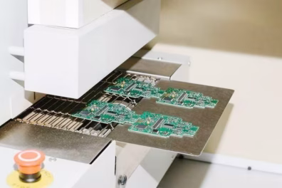
1) Alignment: The SMT stencil is precisely aligned with the solder pads on the bare PCB. Automated vision systems are commonly used to achieve micron-level accuracy.
2) Solder Paste Deposition: A roll of s older paste is placed on the stencil. A metal or polyurethane squeegee blade then moves across the stencil, forcing the paste through the apertures and onto the PCB pads.
3) Separation: After printing, the stencil is slowly and cleanly separated from the PCB. The speed and angle of separation are critical to ensure all the paste releases from the stencil apertures and remains on the pads.
4) Cleaning: The underside of the stencil is regularly cleaned to remove any residual solder paste, preventing smearing and ensuring consistent print quality.
6. Avoiding Pitfalls: Common Stencil-Related Defects
As noted, poor stencil design or usage can lead to significant manufacturing defects. Understanding these and their causes is the first step in prevention.
- Insufficient Solder Paste:This often results from clogged apertures, incorrect stencil thickness for pad size, or a poor area/aspect ratio. It can lead to “opens”(no electrical connection) or weak solder joints.
- Solder Bridging:Too much solder paste, especially on fine-pitch components, can cause adjacent pads to short circuit. This can be due to an overly thick stencil, poorly designed apertures, or misregistration.
- Solder Balls:Small spheres of solder that detach from the main joint, often caused by excessive paste, uneven heating, or poor stencil release.
- Misalignment:The stencil not perfectly aligning with the PCB pads will lead to paste being deposited off-center, causing shorts or opens during component placement. This can be due to human error, machine calibration issues, or stencil warpage.
- Smearing/Paste Slump:Paste spreading uncontrollably, often due to poor stencil separation, excessive paste volume, or inadequate paste viscosity.
Proper stencil design and regular maintenance are crucial for mitigating these issues, ensuring high yield and reliable products.
7. Selecting the Right SMT Stencil
The selection of the appropriate SMT stencil depends on several factors, balancing cost, performance, and specific project requirements.
| Factor | Consideration | Recommended Stencil Type |
|
Production Volume |
Low-to-medium volume, prototyping | Frameless stencils(cost-effective, flexible) |
| High volume, continuous runs | Framed stencils(durability, stability) | |
|
Component Pitch |
Standard pitch(e.g., >0.5mm) | Standard laser-cut stainless steel stencils |
| Fine pitch(<0.5mm), micro-BGAs | Electroformed, nano-coated, or specialized laser-cut stencils with optimized aperture design | |
| Board Complexity | Mixed component sizes, varying paste volumes | Step stencils |
|
Budget |
Cost-sensitive projects | Frameless stencils(lower initial cost) |
| Investment in long-term reliability/efficiency | Framed, electroformed, nano-coated stencils | |
| Desired Print Quality | Maximum paste release, minimal defects | Electroformed, nano-coated stencils |
Consulting with experienced PCB manufacturers and assembly houses like PAA can provide invaluable guidance in making the optimal choice for your specific application.
8. SMT Stencil FAQs
Question1: What is the main purpose of an SMT stencil?
The main purpose is to precisely deposit solder paste onto specific pads of a Printed Circuit Board(PCB) during Surface Mount Technology(SMT) assembly, preparing it for component placement and reflow soldering.
Question2: What is the difference between an SMT stencil and a screen printing stencil?
While both involve pushing paste through openings, SMT stencils are typically made of metal and used for applying solder paste onto PCBs for electronic components. Screen printing stencils, often made of mesh, are generally used for applying ink or paint onto various substrates(textiles, paper, etc.) and are less precise than SMT stencils.
Question3: How often should an SMT stencil be cleaned?
The frequency depends on several factors including the type of solder paste, print speed, component density, and presence of a nano-coating. For optimal results, most automated printers perform an under-stencil wipe after every one to five prints. Manual cleaning may be needed periodically during a run.
Question4: Can I reuse an SMT stencil?
Yes, both framed and frameless stencils are designed for multiple uses. Framed stencils are more durable for high volume, while frameless stencils are used with a reusable frame for lower volume. Proper cleaning and storage after each use are essential to maintain their integrity and print quality.
Question5: Why are laser-cut stencils so popular?
Laser-cut stencils are popular due to their high precision, ability to create complex aperture shapes, smooth aperture walls for excellent paste release, and cost-effectiveness for various production volumes.
Question6: What happens if the aspect ratio or area ratio is too low?
If these ratios are too low(e.g., for very small apertures), it becomes difficult for solder paste to release cleanly from the aperture walls, leading to clogging, insufficient paste deposition, and poor print quality.
Question7: Can one stencil be used for all types of components?
While possible, it’s often not ideal. For boards with a mix of very fine-pitch components and large components, a “step stencil” with varying thicknesses in different areas might be used to optimize paste volume for all components.
9. Summary
SMT stencils are far from simple tools; they are precision instruments critical to the success of Surface Mount Technology PCB assembly. Their ability to accurately deposit solder paste directly impacts the quality and reliability of solder joints, preventing a vast majority of common manufacturing defects. From the robust framed stencil to the specialized step stencil and performance-enhancing nano-coated options, choosing the right type and meticulously designing its apertures and thickness are paramount. By mastering stencil design and best printing practices, engineers and manufacturers can significantly improve yield, reduce rework, and ensure the production of high-quality electronic devices.
Table of Contents
- 1. The Unsung Hero of SMT
- 2. What Exactly is an SMT Stencil?
- 3. Diverse World of SMT Stencil Types
- 4. The Science of SMT Stencil Design: Key Parameters
- 5. The SMT Stencil Printing Process: A Closer Look
- 6. Avoiding Pitfalls: Common Stencil-Related Defects
- 7. Selecting the Right SMT Stencil
- 8. SMT Stencil FAQs
- 9. Summary

Get Your PCB Quote!