What Is a PCB Panel?And What Are Its Advantages?
A PCB panel refers to the consolidation of multiple independent circuit boards onto a single, larger substrate, thereby forming a unified board assembly.At PCBAndAssembly, we handle every stage of your PCB panel project — from DFM review and panel layout optimization to full SMT assembly and depanelization.
Get Your PCB Quote!

Table of Contents
- 1. Qu'est-ce qu'un panneau PCB ?
- Points clés à retenir
- 2. Quand la panélisation des circuits imprimés est-elle nécessaire ?
- 3. Méthode de division du panneau PCB
- 4. Types courants de combinaisons de panneaux de circuits imprimés
- 5. Avantages des panneaux PCB
- 6. Quel est l'objectif du bord de processus du circuit imprimé (détachement) ?
- 7. Règles et méthodes pour les panneaux PCB
- 8. Conception du panneau PCB
- 9. Inconvénients et limites du panneau PCB
- 10. Foire aux questions (FAQ)
- 11. Résumé
1. What Is a PCB Panel?
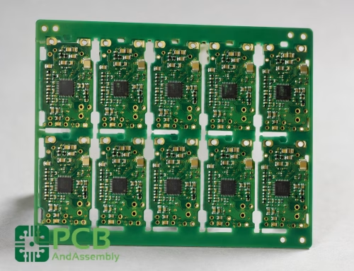
The PCB panel refers to the assembly of several circuit boards onto one large board, in order create a plate.
After the PCB design has been completed, the circuit board and the components must be assembled in the SMT patch assembly line. The SMT factory will specify what size board is best for the assembly line. The tooling used to fix the circuit boards cannot be fixed if the board size is too big or small. What happens if the size of the circuit board is less than the factory’s specifications? The circuit boards will be combined into one single piece. The panel will improve the efficiency and speed of wave peak welders and high-speed patch machines.
PCBs are often “several in one” boards. For example, 2 in 1, 4 In 1, 6 In 1, etc. This means that multiple single boards have been assembled into a large board.
You will see that the largest bottleneck in the SMT line is the “Solder Paste Printing” process. This is because, no matter what size the PCB, it takes almost 25 seconds to print. If the time taken by the expensive fast patching machine or general-purpose patching machine is shorter than the solder paste printing machine, then there will be idleness. Idleness is a loss from the economic perspective.
The speed of the machine is so high that it can punch multiple parts in a second. Some patch machines have multiple nozzles which can punch several parts simultaneously. If there are only one board and a limited number of components on the PCBA, then it shouldn’t take more than 10 seconds to perform all the patching operations. Making the PCB into a jigsaw can improve the efficiency of the patch machine by increasing the number of parts. It is important to “line balance” each device so that it can be used fully.
In some cases, the majority of parts are placed on one side of the PCB while only a few parts are on the opposite side. You can use a mirror board to increase the number on one side, but it will be limited.
Key Takeaways
- Solve the SMT Bottleneck: Solder paste printing takes ~25 seconds regardless of board size. Combining multiple PCBs into one panel multiplies the components processed per cycle, balancing the SMT line and eliminating costly machine idleness.
- Cut Material Waste Significantly: Small or irregularly shaped PCBs often leave large areas of substrate unused. An optimized panel layout can dramatically reduce this waste — the cost difference between a poorly utilized panel and a well-optimized one can be very large.
- Pick the Right Depanelization Method: V-cut is fast and low-cost for rectangular boards; tab routing suits irregular shapes and edge-mounted components. Choosing the wrong method can crack ceramic capacitors or damage fine-pitch ICs during board separation.
- Design Rules Are Non-Negotiable: A minimum 3.5 mm board-to-edge margin, at least 1.0 mm PCB thickness for V-cut, and a square 2×2 or 3×3 array are all required. Violating any one of these can cause warpage, misaligned solder paste, or machine collisions on the production line.
2. When Is PCB Panelization Required?
PCB panelization becomes necessary in several practical scenarios:
- When individual PCBs are smaller than the SMT line’s minimum board-size requirement (typically less than 80×80 mm).
- When CNC machines or pick-and-place equipment would be under-utilized processing one tiny board at a time, since these machines consume nearly the same power and setup time regardless of board size.
- When high-volume orders (tens to hundreds of thousands of units) make simultaneous multi-board processing economically essential.
- When different small board designs share the same layer count and production process and can be combined to share setup costs.
By mounting smaller boards onto a larger panel, manufacturers significantly enhance the convenience and efficiency of the production process while enabling simultaneous quality control across all boards in the array.
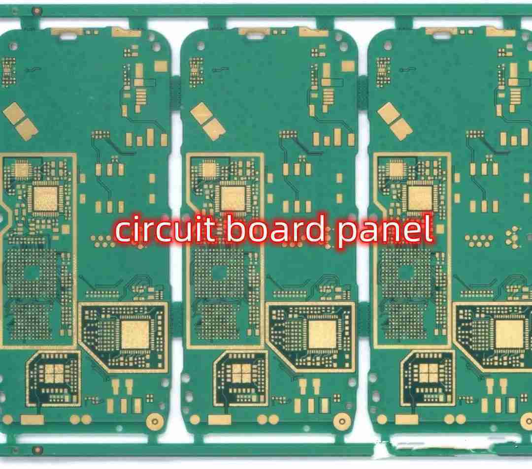
3. PCB Panel Division Method
The panels must be assembled during the design phase. After the final processing, we need to separate plates. Three traditional methods are used.
1) V-CUT
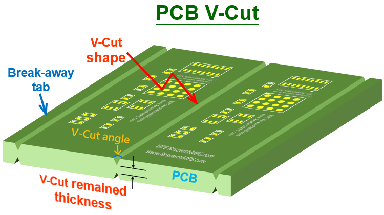
When several plates are combined (or if the same plate is used), the PCB cuts a V shape slot into the plates. It can come off when used. This is the most common method today.
Features: A V-shaped groove is suitable for PCBs that have a straight edge. This includes rectangular PCBs. It is the most popular choice for SMT board because of its neat edge and low processing cost.
2)Solid Tab Panelization
Solid tabs (no perforations) connect boards for maximum structural rigidity. Depanelization requires a dedicated routing machine, laser cutter, or hook-blade tool.
- Best for: Applications where maximum panel strength during assembly is critical.
- Limitations: Requires specialized depanelization tools; routing can generate dust and vibration.
3)Tab Routing (Mouse Bite / Stamp Hole)
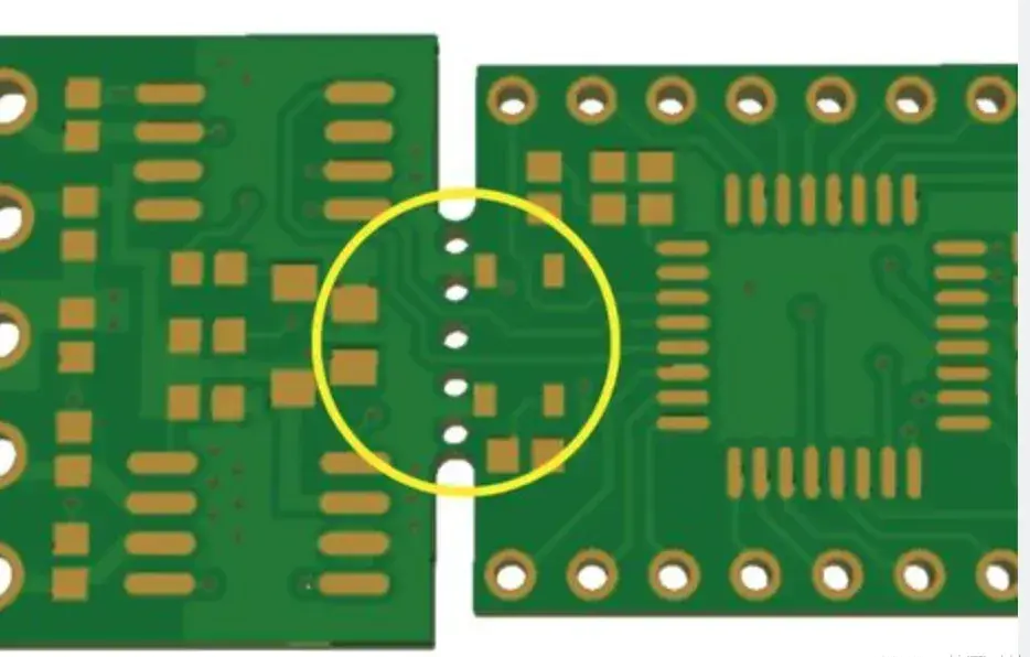
The PCB is pre-cut (routed) from the array and held in place by small perforated tabs — also called “mouse bites” or “stamp holes.” After assembly, tabs are broken or routed away.
- Best for: Irregular, non-rectangular board shapes; boards with edge-mounted or overhanging components.
- Advantages: Flexible for complex shapes, cleaner control over breakout location.
- Limitations: Leaves small nubs (burrs) that may need sanding; slower routing time than V-cut.
- Tab spacing: 5-hole perforated tabs should be spaced every 2–3 inches; 3-hole tabs every 1.5 inches.
- Clearance: Maintain at least 1/8 inch between parts/traces and the tab; 1/4 inch for large ceramic capacitors.
V-Cut vs. Tab Routing — Quick Comparison
| Factor | V-Cut | Tab Routing |
| Board Shape | Square / Rectangular only | Any shape, including irregular |
| Speed | Fast (machine scoring) | Slower (router time) |
| Edge Quality | Rough throughout | Small nubs, can be sanded smooth |
| Edge Components | Not suitable for close-edge components | Suitable, tabs placed away from components |
| Material Waste | Lower waste | Slightly more waste from routing |
| Stress on PCB | Snapping can stress edges | Cleaner separation, lower stress |
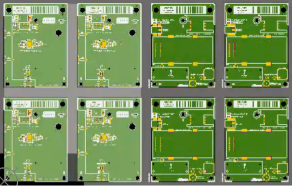
4. Common PCB Panel Combination Types
The arrangement of individual boards within a panel is not one-size-fits-all. Three common combination strategies are used depending on production goals:
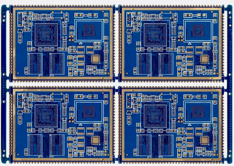
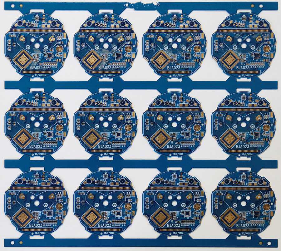
AAAA Combination (Same-Board Array)
The most commonly used method: multiple copies of the identical PCB are arrayed together. Compatible with virtually all fabrication processes, maximizes throughput, and simplifies stencil design because pad orientation is consistent across all boards. Highly recommended as the default panelization strategy.
ABCD Combination (Mixed-Order Panel)
Different PCB designs are combined on the same panel — often used by PCB manufacturers to fill panel space and reduce material waste. Benefits include increased production efficiency and lower per-order cost. Downside: quality issues on one board design can affect the entire panel.
ABAB Combination (Alternating Design)
Two or more related PCB designs (from the same product) are alternated on the panel. Suitable for medium-sized electronic products with 3–5 small, interconnected boards. Less common but useful when component placement directions complement each other.
5. Advantages of PCB Panels
1) Increase the Efficiency of SMT Production
Which is faster, 6pcs or 1pcs? Panel increases our production efficiency but also allows for faster delivery. Faster delivery means a shorter time to market and a competitive advantage.
The panel design and the process side design eliminate the need to open treatment equipment. This allows you to reduce the time required for prenatal preparation, so you can deliver faster.
The number of transmission boards and the cycle frequency can be decreased by processing multiple PCBs into one large PCB at a time. This allows for the production of more circuits in less time. It also improves the efficiency and lowers the price of the PCB. This is important, especially for large-scale electronics manufacturers.
2) Maximize Plate Utilization Rate
It is possible that the PCB design has created many unusable boards.
As the figure below shows the cost difference between the two methods of paneling is very large.
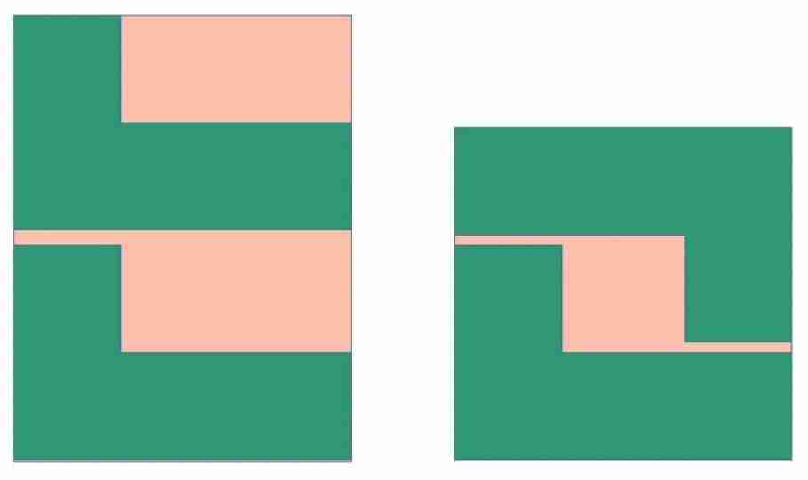
We can reduce costs and waste by combining small or irregularly-shaped PCBs.
It is important to consider this when pursuing production processes that are cost-effective.
3) Reduce Production Difficulty
The production process is made easier by reducing the complexity of the PCB to a simpler structure. It is important to improve production efficiency and ensure product quality.
Multiple boards can be combined if the company is small, the projects are numerous, the number of layers, the production and processing technologies are the same. The board factory may charge a combined fee, but it will be much less expensive than processing multiple projects separately.
The patch factory will only do one project if there are multiple projects to be made into Boys. This saves a lot of money on the cost.
6. What Is the Purpose of the PCB Process Edge (Break-Away)?
Many people call this break-away or coupon because it can be broken directly. It is similar to the discount coupons in convenience stores. It is not recommended that the board edges are broken by hand for quality reasons. To reduce the stress created when board edges are broken, machine equipment (Scoring and Router) can be used to remove them. This will help to prevent tin cracking on parts or board.
PCB board edges are designed to aid in PCBA assembly. SMT is a highly automated production line, with the board being transported via belts and chain. It was a clever idea. The board edge’s main purpose is to transport this board with these belts and chain.
You can, of course, leave some space around the board if you wish. It is recommended to leave at least 5.0 mm around the board because the iron chain for the reflow oven needs to be positioned deeper. This allows you to avoid designing the board edge.
The edge of the PCB can also be used for other purposes:
Place tooling holes: After the SMT process, “tooling holes” may be used to help position the board for ICT or FVT tests. This will prevent the needle bed from moving and the test point.
Detect the position of the circuit board: Each machine in the SMT line has a sensor that detects whether there are any subsequent boards to make sure only one panel works. The patchwork of the previous board will not be completed, and it will cause the other panel to crash into the first panel, causing chaos. Some single boards will have a hollowed-out appearance at the location where the SMT production lines sensor detects them, which is usually the upper left corner at the front edge. The edge of the board is now a good way to detect solids by the sensor.
Positioning optical points: If space is limited, you can place the fiduciary marks at the edges of some boards. However, it’s recommended to also have the positioning points near the fine foot of the board on the parts’ tray to improve the accuracy of the patch.
7. Rules and Methods for PCB Panel
1) Understand the Panel’s Maximum and Minimum Sizes
The maximum and minimum sizes of the panels should be clearly defined according to the requirements of each patch factory. The maximum size depends on the factory’s processing capacity. Generally, PCBs less than 80X80mm require a panel.
2) Panel Meets DFM DFA Requirements
After the fixture, the panel must be fixed and not easily deformed. The surface flatness of the PCBA patches processing shall be met by the split grooves that are between the panels.
3) Reduce the Stress on the Components
The PCB panel should be designed to avoid component cracking due to segmentation stress. Pre-engraved lines on the panel can reduce the deformation and warping of the panel.
4) Design the Plate as Closely as Possible to a Square
A 2×2 or 3×3 symmetric panel array is the ideal configuration. Square panels are easier to handle, less prone to warping, and more efficiently processed on automated equipment. Mirror-board layouts are not recommended unless absolutely necessary.
5) Avoid Profile from the Edge Connector
Rotating the panel + edge of the process is the solution to the problem when the outline of the panel-side connector exceeds the interference. This will prevent poor quality collision parts being transmitted or handled after welding.
6) Make Sure That the Bottom Point of the Large Plate Has a Margin of at Least 3.5 mm
The panel design must be such that the edge of the large baseplate should be at least 3.5 mm away from the plate. (The minimum distance of the PCB is 3.5 mm). Also, the diagonal bases of the large baseplate and the points of the front or back of the panel cannot be symmetrical. This can prevent PCBs being reversed into the machine by the identification function.
7) The Thickness of the PCB Plate Is Not Less Than 1 mm
For V-cut panels, PCB thickness below 1.0 mm compromises the glass fiber cloth support skeleton at the V-groove, reducing panel rigidity and increasing the risk of warpage during reflow. Panels below this thickness may require a dedicated furnace carrier.
8) The Gold Finger Edge Cannot Be Added to or Connected With the Process Edge
If there is a gold finger on a PCB, it is usually placed on the outside of the plate in the direction opposite to the splint. The edge of the gold finger cannot be added or connected to a process edge.
9) Balance Number of Sub-Boards vs. Tolerance
Too many sub-boards on a single panel can accumulate dimensional tolerances, making it impossible to meet solder paste printing accuracy standards. For thin PCBs, excessive paneling increases board warpage. If a full-process carrier (SMT pallet) is required to control warpage, the added cost must be factored into the panel design decision.
8. PCB Panel Design
Multiple factors must be taken into consideration in the design of a PCB panel.
In order to meet the requirements of the PCB panel design, it is important to consider other factors.
1) Consider the Product’s Characteristics
First, the analysis of product characteristics should be comprehensive, including circuit layout, power consumption, and signal transmission.
It is possible to operate the panel system with greater stability and reliability by avoiding the performance degradation and interference caused by a complex circuit structure.
2) Balance the Plate Utilization Rate with Production Efficiency
The production capacity and efficiency should be taken into consideration when selecting the number of panels and the method to use. This will ensure that there are no additional bottlenecks in the manufacturing process.
A good layout can reduce waste and have a positive effect on the environment and sustainable development.
3) Ensure Product Reliability and Safety
Special attention is given to the effect of panels on signal integrity and circuit stability.
Avoiding the crossing of and interference with signal lines can maximize the performance of the circuit.
In order to design high-frequency circuits or sensitive components that can operate reliably and stably under different working conditions, a more precise layout and analysis is required.
4) Consider the Manufacturing Costs and Processing Difficulties of SMT Production
It is also important to consider the manufacturing costs and processing difficulties of SMT.
To avoid creating unnecessary problems, the pooling scheme must be coordinated with SMT’s production process.
A comprehensive cost evaluation, including labor, material and equipment costs, is also required to determine whether the panel design can be made cost-effectively.
We work closely with the production line during the entire PCB panel design process to ensure the design scheme is compatible with the needs of the product.
9. Disadvantages and Limitations of PCB Panel
Adds a Depanelization Step
After all PCBA assembly, every panel must still be separated into individual boards. This adds a process step, increases total working hours, and introduces additional handling opportunities where boards can be scratched, dropped, or cracked — especially for delicate boards with fine-pitch BGAs.
Panel Count Must Be Carefully Balanced
If a PCB has many fine-pitch components or dense layouts, too many boards per panel will accumulate dimensional tolerance errors that exceed the solder paste printing accuracy specification, causing misaligned paste deposits and downstream soldering defects.
Thin PCBs Are More Prone to Warpage
For PCBs thinner than 1.0 mm, increasing panel width increases the risk of bow and twist. Wide, thin panels may sag in the reflow oven, causing component misalignment. A full-process furnace carrier can mitigate this but adds cost and reduces throughput.
10. Frequently Asked Questions (FAQ)
Q: What is the difference between a single PCB and a PCB panel?
A single PCB is manufactured and processed alone. A PCB panel (array) is a larger sheet containing multiple individual PCBs interconnected, processed together for manufacturing efficiency, and separated after assembly.
Q: Why is PCB panelization considered cost-effective?
Panelization reduces machine setup times, optimizes material usage, lowers per-board labor costs through collective handling, and increases throughput. For high-volume orders, cumulative savings are substantial.
Q: What are the common depanelization methods?
V-scoring (snapping along pre-cut grooves) and tab routing (breaking or routing away perforated tabs/mouse bites) are the two primary methods. Solid tab routing with dedicated cutting tools is a third option for high-strength panels.
Q: Can flexible PCBs be panelized?
Yes. PCB panelization applies to rigid, flexible, and rigid-flex boards. The efficiency and cost benefits are the same, though specific design clearances and breakout methods for flexible materials may differ.
Q: What is the minimum panel thickness recommended?
A minimum PCB thickness of 1.0 mm is recommended for V-cut panels. Thinner boards compromise the glass fiber support at the groove and increase warpage risk.
11. Summary
PCB panel design in general is a complex, comprehensive process that requires engineers to think holistically at various levels.
By carefully designing, you can not only improve the production efficiency and reduce costs but also ensure the reliability and performance of your product.
The design of PCBs will continue to be important in the future, as science and technology continues to develop and the manufacturing industry grows.

Get Quote Free