Common PCB Inspection Methods and Techniques: A Detailed Overview
This is a guide about PCB inspection, helping you understand common inspection methods, typical defects, and how to conduct visual checks and related tests. It will also teach you how to choose the right inspection solution.
Get Your PCB Quote!
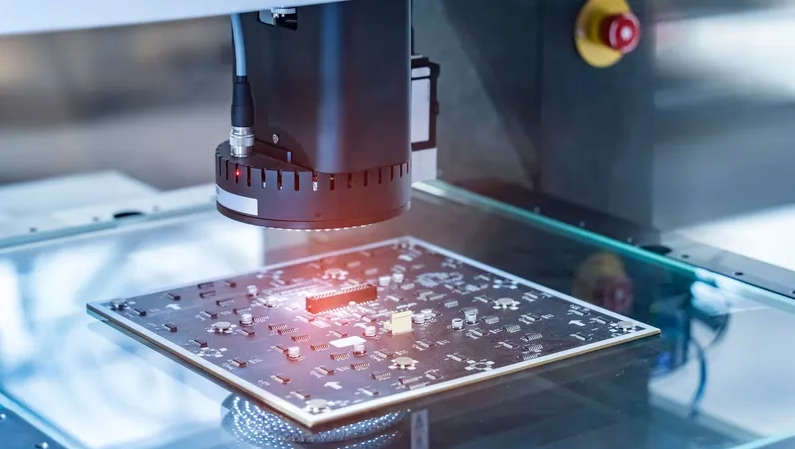
Table of Contents
1. Introduction
As electronic assemblies grow increasingly complex, the ability to detect manufacturing defects early has become a defining factor in product quality and cost efficiency. Industry data from the IPC indicates that assembly-related defects account for nearly 70% of failures in electronic products, while findings from IEEE suggest that catching defects at early production stages can cut rework expenses by 30 to 50 percent.
These figures underscore why a structured approach to quality control is no longer optional — it is a fundamental requirement in modern electronics manufacturing. This guide examines the most widely used PCB inspection methods, the equipment each relies on, their respective strengths and constraints, and how emerging technologies are reshaping the field.
Key Takeaways
- Early detection significantly reduces rework costs and prevents downstream field failures.
- No single method is sufficient; combining MVI, AOI, AXI, electrical testing, and functional testing provides the most comprehensive coverage.
- AOI and AXI serve complementary roles — AOI targets visible defects while AXI is indispensable for hidden solder joints and internal structures.
- ICT offers high fault coverage for high-volume production; flying probe testing provides flexibility for prototypes and lower volumes.
- AI, machine learning, and 3D inspection are driving measurable improvements in detection accuracy and operational efficiency.
- Compliance with standards such as IPC-A-610 ensures objective, consistent quality evaluation across the supply chain.
2. Core PCB Inspection Methods
Quality assurance across a PCB production line typically involves multiple inspection techniques applied at different stages. The selection of any given method depends on the board type, the production phase, and the nature of the defects being targeted.
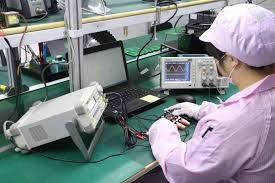
2.1 Manual Visual Inspection (MVI)

Manual Visual Inspection is among the earliest and most accessible forms of PCB quality control. Trained operators examine boards directly — often with the aid of magnification tools — to identify surface-level anomalies such as poor solder joints, component misalignment, trace damage, polarity errors, or contamination.
Although it appears straightforward, MVI remains a relevant first line of defense in many production environments because of its adaptability and the human eye’s capacity to recognize subtle or unfamiliar defect patterns.
Equipment: Magnifying lamps, stereo microscopes, bore scopes, and specialized lighting.
Advantages:
- Highly adaptable to varying board designs without programming overhead
- Capable of identifying a broad range of cosmetic and obvious defects
- Low setup cost, suitable for low-volume or prototype environments
Limitations:
- Results vary with operator fatigue, skill level, and experience
- Time-intensive and impractical for high-volume production lines
- Cannot inspect concealed solder joints, such as those beneath BGA or QFN packages
- Susceptible to both missed defects and false positives
2.2 Automated Optical Inspection (AOI)
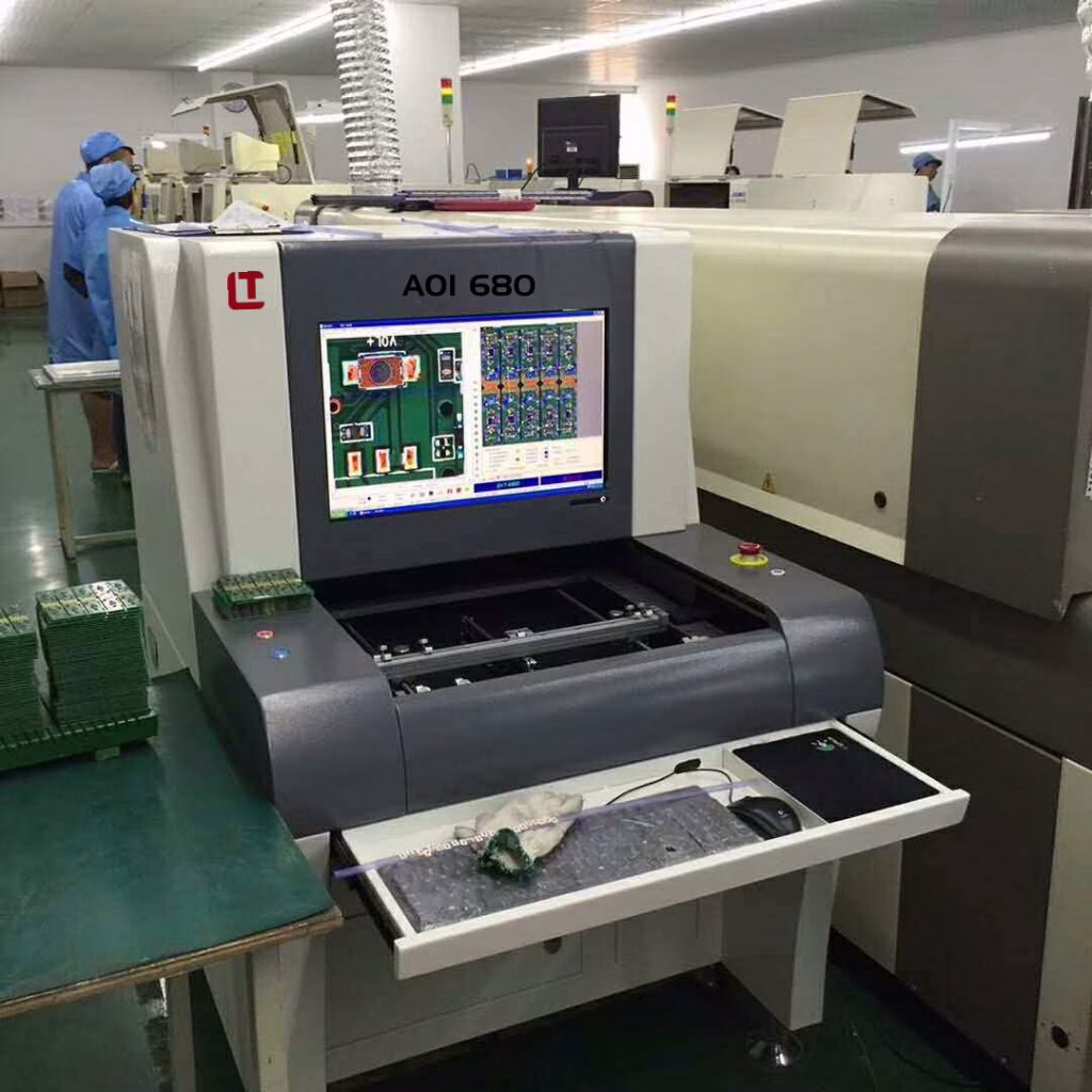
AOI represents a substantial advancement over manual methods. High-resolution camera systems combined with image-processing software scan assembled PCBs and compare captured images against a reference standard or design specification. This allows for rapid, consistent detection of a wide range of surface-level defects.
AOI is commonly deployed after solder paste application, component placement, and reflow soldering. Modern systems can inspect thousands of components per minute, making them well-suited to high-volume manufacturing.
Equipment: 2D and 3D digital cameras, LED-based illumination arrays, and advanced image-processing software.
Advantages:
- High throughput and consistent results, eliminating operator subjectivity
- Detects a wide array of defects including shorts, opens, missing or misplaced components, polarity errors, and solder joint issues
- Reduces labor costs and supports efficient high-volume workflows
Limitations:
- Cannot inspect solder joints hidden beneath BGA, QFN, or similar packages
- Variations in component finish or lighting can generate false calls
- Requires significant programming investment for each new board design
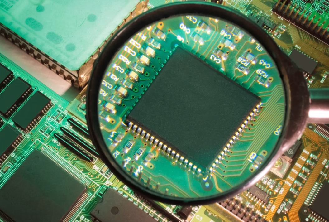
2.3 Automated X-Ray Inspection (AXI)
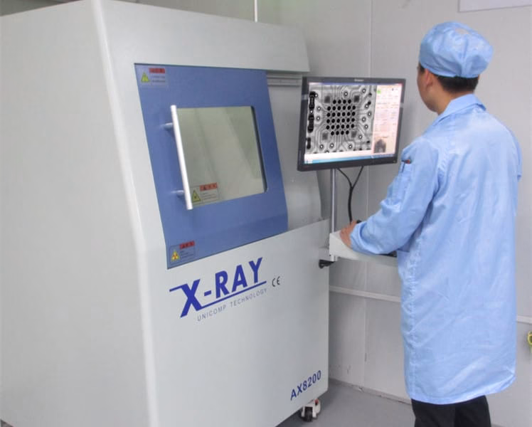
AXI is the primary method for inspecting defects that are entirely hidden from optical view. X-ray energy penetrates PCB materials and components, producing images that reveal solder joint integrity, internal layer structures, and other features inaccessible to cameras.
Both 2D and 3D AXI systems exist. Three-dimensional systems construct volumetric images that allow for comprehensive analysis of complex assemblies, including those using Ball Grid Array (BGA), Chip Scale Package (CSP), and Quad-Flat No-lead (QFN) components.
Equipment: X-ray sources, imaging detectors, and dedicated software for image reconstruction and defect analysis.
Advantages:
- Essential for evaluating hidden solder joints under BGA, CSP, and QFN packages
- Identifies internal defects such as voids, solder bridging, and shorts between internal layers
- Provides detailed analysis of solder joint characteristics including fillet shape and voiding
Limitations:
- Higher equipment cost relative to MVI and AOI
- Slower inspection throughput than AOI
- Interpreting complex X-ray images requires specialized training
- Radiation safety protocols must be observed
2.4 Electrical Testing: In-Circuit Test (ICT) and Flying Probe
Electrical testing methods verify that PCB circuits are electrically intact and that components function within specified parameters. Unlike visual inspection methods, these tests confirm connectivity and component performance rather than appearance.
In-Circuit Test (ICT)
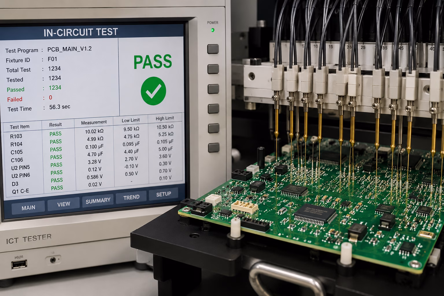
ICT employs a bed-of-nails fixture — a custom array of test probes that simultaneously contact designated test points on the PCB. The system measures individual component values such as resistance, capacitance, and inductance, and validates trace and connection integrity. ICT is well-suited to high-volume production where upfront fixture costs are offset by rapid test execution.
Equipment: Custom bed-of-nails fixture, test generation software, and dedicated test system hardware.
Advantages:
- High fault coverage for manufacturing defects
- Fast execution once the fixture and program are in place
- Enables precise fault localization, simplifying rework
Limitations:
- Custom fixtures are required for every unique PCB design, adding cost and lead time
- Requires dedicated test pads that consume board real estate
- Access constraints on high-density, fine-pitch boards
- Does not verify full circuit functionality in operating conditions
Flying Probe Test
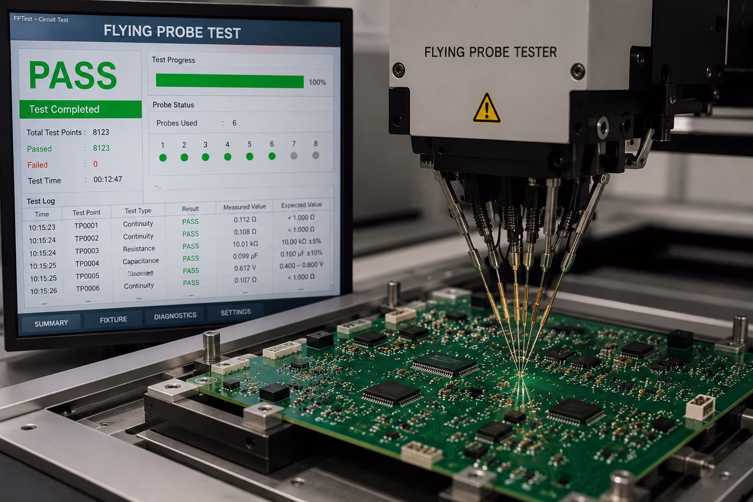
The flying probe test uses robotic probes that traverse the board surface to make contact with individual test points. Because no custom fixture is required, this method is highly flexible — particularly well-suited to prototype development, engineering changes, and low-to-medium volume production.
Equipment: Typically four to eight robotic probes, integrated vision systems for positioning, and test programming software.
Advantages:
- No fixture costs, reducing both upfront investment and lead time
- Easily adapted to different board designs and design revisions
- Can access fine-pitch components
Limitations:
- Slower than ICT for large production volumes
- May provide lower fault coverage than ICT on certain board types
- Limited capability for testing power-on functionality
2.5 Functional Testing
Functional testing is typically the final stage of PCB inspection. Rather than examining individual components or connections in isolation, it evaluates the assembled board as a complete system under conditions that closely simulate its intended operating environment. This confirms that hardware, firmware, and software interactions perform as designed.
Equipment: Custom test fixtures, power supplies, oscilloscopes, multimeters, load circuits, and specialized software for automated test sequences and data logging.
Advantages:
- Validates the PCB as a functioning system, not just as individual components
- Catches failures invisible to other methods, such as timing issues or cross-component interactions
- Provides direct confidence in field performance
Limitations:
- Does not isolate individual component failures; root cause diagnosis can be complex
- Test routines and fixtures can be time-consuming to develop
- Defects found late in production are costlier to rework
Need PCB Manufacturing or Assembly?
Get a free quote within 24 hours. We specialize in prototype-to-production PCB/PCBA for hardware teams worldwide.
3. Inspection Method Comparison
The table below summarizes the primary characteristics of each method to aid in selection decisions.
| Method | Primary Focus | Key Advantages | Key Limitations | Best Suited For |
| Manual Visual (MVI) | Visible surface defects | Flexible, low cost, no programming | Subjective, slow, cannot inspect hidden joints | Prototyping, low volume, initial checks |
| Automated Optical (AOI) | Visible manufacturing defects | Fast, consistent, high throughput | Cannot inspect hidden joints; programming overhead | High-volume post-solder inspection |
| Automated X-Ray (AXI) | Hidden joints and internal structures | Inspects BGAs/CSPs; reveals internal flaws | High cost, slower speed, complex interpretation | Complex boards with BGA or CSP components |
| In-Circuit Test (ICT) | Electrical shorts, opens, component values | High fault coverage, precise diagnosis | Expensive fixtures, requires dedicated test pads | High-volume production, mature designs |
| Flying Probe Test | Electrical shorts, opens, component values | No fixtures, flexible, low initial cost | Slower than ICT; lower coverage in some cases | Prototyping and low-to-medium volume |
| Functional Test | Overall system performance | Verifies end-use behavior | Late detection; complex fault diagnosis | Final quality gate before shipment |
4. Emerging Trends and Advanced Technologies
The PCB inspection field continues to evolve in response to increasingly complex board designs and ever-tighter quality requirements. Several technological advances are expanding what inspection systems can detect and how efficiently they operate.
4.1 Three-Dimensional Inspection
Two-dimensional inspection has inherent limitations when evaluating solder volume, component coplanarity, or complex solder joint geometry. Three-dimensional AOI systems address this by using laser triangulation or structured light projection to measure component height and solder paste volume with greater accuracy. Similarly, 3D AXI systems generate volumetric images that provide an unobstructed view of internal structures, enabling more comprehensive analysis of hidden assemblies.
4.2 Artificial Intelligence and Machine Learning
AI and machine learning are increasingly integrated into both AOI and AXI platforms. Rather than relying solely on fixed rule-based thresholds, these systems learn from large datasets of confirmed good and defective boards. The result is more accurate defect classification, reduced false call rates, and improved adaptability to new component types or process variations. According to a 2024 study by Prismark Partners, AI-powered inspection systems have demonstrated reductions in false call rates of up to 60 percent, meaningfully improving throughput and reducing manual verification burden.
4.3 Digital Traceability and Smart Manufacturing
In high-reliability industries such as medical devices and electric vehicles, the ability to trace every board through each stage of production is as important as the inspection outcome itself. Modern inspection platforms increasingly support network connectivity and integration with Manufacturing Execution Systems (MES), enabling automatic data logging, image archiving, and the creation of a digital record for every inspected unit. This supports recall management, process optimization, and regulatory compliance across global supply chains.
4.4 Integrated Inspection Workflows
Rather than treating each inspection method as a standalone operation, manufacturers are moving toward integrated workflows in which data from AOI, AXI, SPI (Solder Paste Inspection), and electrical testing is aggregated and analyzed centrally. This holistic view enables faster identification of systemic process issues and provides a more complete picture of overall board quality than any single method can offer.
5. Choosing the Right Inspection Approach
Selecting appropriate inspection methods is a strategic decision shaped by several interdependent factors. No single technique is universally optimal; the best approach depends on the specific production context.
5.1 Production Stage
Inspection needs differ at each phase of assembly. Solder Paste Inspection (SPI) is applied before component placement. AOI is most effective after reflow soldering. AXI is deployed when complex packages require subsurface analysis. Functional testing serves as the final gate before shipment.
5.2 PCB Complexity and Component Type
Simple single-layer boards may be adequately served by MVI and basic electrical testing. High-density boards featuring fine-pitch BGAs, CSPs, or multilayer structures require AOI and AXI as a baseline, often supplemented by ICT or flying probe testing.
5.3 Production Volume and Cost Constraints
For high-volume production, the consistent throughput of AOI and the fault-coverage efficiency of ICT justify their higher setup costs. For prototype runs and low-to-medium volume production, flying probe testing and MVI provide the necessary flexibility without the overhead of custom fixtures.
5.4 Required Fault Coverage
Define which defect categories are most critical for the product. If hidden solder joints are a primary concern, AXI is non-negotiable. If comprehensive electrical verification is required, ICT or flying probe testing is essential. In practice, layering multiple methods across the production process delivers the broadest fault coverage and the greatest protection against field failures.
About PCBAndAssembly
Time is money in your projects – and PCBAndAssembly gets it. PCBAndAssembly is a PCB assembly company that delivers fast, flawless results every time. Our comprehensive PCB assembly services include expert engineering support at every step, ensuring top quality in every board. As a leading PCB assembly manufacturer, we provide a one-stop solution that streamlines your supply chain. Partner with our advanced PCB prototype factory for quick turnarounds and superior results you can trust.
6. Relevant Industry Standards
Adherence to recognized standards ensures that inspection criteria are consistent, objective, and aligned with customer expectations across global supply chains.
- IPC-A-610 — The most widely used visual inspection standard, defining target, acceptable, and defect conditions for electronic assemblies. For example, BGA solder joint void size is typically limited to 25% of the ball diameter for Class 3 (high-reliability) products.
- IPC-J-STD-001 — Addresses materials, processes, and workmanship requirements, complementing the visual criteria of IPC-A-610.
- IPC-6012 — Sets performance and qualification requirements for bare PCBs prior to assembly.
- MIL-PRF-31032 — Applies to defense electronics, mandating stricter validation including thermal shock testing, mechanical reliability testing, and micro-sectioning of vias.
7. Frequently Asked Questions
What are the most commonly detected PCB defects?
The most frequent defects include solder bridges, open circuits, insufficient solder, voids in solder joints, component misalignment or omission, incorrect polarity, and trace damage. Hidden defects such as voids beneath BGA packages are particularly critical in high-reliability applications.
Can a single inspection method guarantee defect-free boards?
No. Each method has inherent blind spots — MVI cannot detect hidden joints, AOI cannot see inside packages, AXI may not detect all electrical failures, and functional testing may not isolate individual component faults. Comprehensive quality assurance requires a layered strategy combining complementary methods.
How do IPC standards inform the inspection process?
Standards such as IPC-A-610 provide objective, widely accepted criteria for classifying solder joint quality, component placement acceptability, and workmanship. They align expectations between manufacturers and their customers, reduce quality disputes, and enable consistent evaluation across global supply chains.
When is X-ray inspection strictly necessary?
X-ray inspection becomes essential whenever the board contains components whose solder joints are not accessible to optical systems. BGA, CSP, and QFN packages are the most common examples. For safety-critical applications in aerospace, automotive, or medical device manufacturing, AXI is typically a mandatory step regardless of component type.
Summary
Effective PCB inspection is not a single-step activity — it is a multi-layered quality strategy that spans every stage of the manufacturing process. From early manual checks and high-speed automated optical scans to subsurface X-ray analysis and final functional validation, each method contributes a distinct and valuable layer of defect detection.
As component density increases and packaging formats grow more complex, the role of advanced technologies — particularly 3D inspection, AI-driven defect classification, and digital traceability — will continue to expand. Manufacturers who invest in the right combination of inspection methods, guided by production stage, board complexity, volume, and fault coverage requirements, are best positioned to deliver reliable electronics while controlling the cost of quality.

Get Quote Free