How to choose HDI PCB materials and optimize costs?
Discover everything about HDI PCB in this complete guide. Learn about fabrication, cost, manufacturing, and more in HDI circuit boards.
Get Your PCB Quote!

Table of Contents
High-performance electronic devices are in demand for their compact size and superior functionality, and all of it is owed to circuit board technologies. Among these, HDI PCB ensure complex designs and high-speed interconnects. This book tries to give you all the information about the HDI circuit boards-from stability methods to costs considerations.
1. What Defines an HDI PCB?
A high-performance board has ultra-fine lines and tightly packed components. There is this kind of detailing so that there can be more connections within smaller footprints. These boards can be layered by advanced techniques and have reliable electrical paths, making them essential in contemporary devices. HDI PCB technology helps pack more wiring into smaller spaces, perfect for today’s compact electronics.
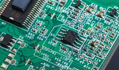
2. Core Technologies and Structure
These circuit boards layers include microvias, blind vias, and buried vias. The pathways connect layers without occupying excessive space. This arranged set of vias allows engineers to achieve ultra-dense interconnections relative to signal integrity. The advanced layering thus makes the multi-block integration possible. Advanced HDI PCB fabrication techniques are essential for achieving miniaturisation without sacrificing reliability.
3. Process of Manufacturing Made Easy
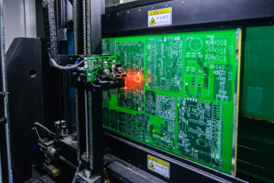
Such complex boards require precision at every step. Manufacturers first finish layer stack-up design. Microvia PCB is then drilled with advanced laser equipment. In the next step, copper plating gets done so that the electrical pathways get strengthened. After plating, the board may be imaged, etched, and laminated. Each step must therefore be precise in terms of connectivity and performance.
4. Materials Selection
Dielectrics and copper weights essentially govern electrical performance, heat tolerance, and mechanical stability. HDI PCB manufacturers need to choose their materials assuring a trade-off between signal requirements and thermal management issues. Very high-frequency uses would require special substrates for the least amount of signal loss.
5. Applications for HDI Circuit Boards
HDI circuit boards are used in smartphones, tablets, and wearables because of their diminutive form factors. Telecom-equipment and networking hardware also rely on them to function at high-speed data transfer. Apart from automotive sensors, medical devices, and any other types of applications needing miniaturization and reliability for manufacturers who produce HDI PCB board.
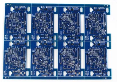
6. Manufacturing and Sourcing
As far as quality and repeatability are concerned, production by a reliable HDI PCB supplier. The experience, certification, and production capabilities of the manufacturers should be reviewed when evaluating them. For a project involving quick prototyping or very fine dimension-based applications, the choice of the manufacturer impacts lead time and cost efficiency. HDI PCB electronics manufacturingenables the creation of complex and space-saving layouts for modern applications
7. Cost Factors Explained
The price of an HDI board can vary depending on several factors, like its size, how many layers it has, the type of via used, the materials selected, and how many units are being ordered. Microvias PCB and finer features usually cost more. However, the benefits sometimes justify that expense in terms of performance enhancements and space savings. It is essential to balance the somewhat ambitious designs with the real world of budgets.
8. Quality Assurance Practices
High density interconnect PCB require stringent testing. Early defect detection is possible through automated optical inspection, flying probe testing, and X-ray analysis. Through such tough QA methods, manufacturers make sure that the boards can satisfy their electrical performance requirements as well as having long-term reliability.
9. Design Best Practices
Good design does great to avoid weak points and signal interruptions. Engineers need to maintain trace widths, spacing, and via placements properly. Careful planning for thermal relief and impedance matching is crucial. Thanks to advanced techniques, one can build tiny, powerful boards without sacrificing performance. Every interconnect PCB is designed to keep signals clear and reliable, even across multiple layers.
10. Innovation in PCB Technology
The trend towards smaller features and more layers continues. Passive components embedded in the circuit and flexible substrates are gaining acceptance in the industry. In the context of the proliferation of 5G, AI, and IoT devices, the demand for advanced HDI solutions will probably rise. HDI printed circuit board technology allows for higher wiring density and improved signal performance in compact electronic devices.
11. Budget Tips
Prototype testing before full production can save one from very costly mistakes. The HDI PCB cost varies depending on layer count, material selection, and production volume. Design changes during low-volume runs are far less expensive. Also, try to negotiate volume discounts or standardized layer counts to decrease per-unit costs. Designing for manufacturability is facilitated by early collaboration with the manufacturing partner.
12. Future Outlook
With increasing consumer expectations, the less size and faster speed of electronic gadgets required become. Engineers are traversing into areas of 3D stacking, embedding components, and flexible HDI formats. It may be interesting that gadgets get thin with lots of integrated functions.
13. HDI PCBFAQs
They use smaller vias, more layers, and finer traces for compact layouts and superior performance.
Yes, many manufacturers are prepared for both prototyping and full production keeping the same quality.
Yes, it does. Special substrate materials will help with signal integrity and decrease thermal problems, more so in the case of high-frequency designs.
Being small in size, these can fit smart devices, equipment within telecommunication, automobile electronics, medical instruments, and more.
Prototyping, layer count adjustments, and negotiating volume pricing are some options here. Early engagement with manufacturers will also help to optimize the design.
Usually, inspection procedures to be carried out are the optical inspection, electrical testing, and X-ray analysis for finding any defects before these boards are assembled into the final devices.
Yes. Most boards in these technologies are RoHS compliant or have lead-free finishes and are increasingly moving toward environmentally friendly manufacturers.
Yes. Embedded passives and flex PCB elements are more and more used to achieve more efficient designs.
14. Summary
This document has gone over everything, from HDI PCB manufacturing process to material choices, cost factors, and quality control techniques in high-density interconnect production. By understanding these aspects of HDI circuit boards, engineers would be better able to go forward designing smarter, faster, and more efficient electronics.

Get Quote Free