From Design to Production: PCB Board Fabrication Explained by Leading Manufacturers
Explains PCB fabrication steps: design verification, copper patterning, drilling, testing, and choosing a reliable manufacturer for quality boards.
Get Your PCB Quote!
Table of Contents
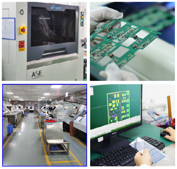
PCBs are the crucial infrastructure for today’s electronics, including medical equipment, TVs, smartphones, or more. PCB board fabrication requires multiple precise steps to convert a design idea into a working product. Top industry manufacturers have perfected the fabrication process to deliver high-quality and efficient results with reliable outcomes. This blog examines the process of transforming design into production while providing insights into the methods and technologies that define the fabrication.
Understanding PCB Board Fabrication
The essential process of the fabrication creates a physical circuit board by etching conductive pathways onto a non-conductive substrate to connect electronic components. The assembled electronic circuits rely on these boards to operate their devices according to design specifications. Fabrication process starts with a design phase and concludes with a completely assembled board ready to integrate with an electronic device.
The first step in the process is creating a schematic which serves as a detailed plan for electrical connections and circuit components. The digital file functions as the complete guide for the fabrication process to ensure all layers, traces, and holes meet the precise design specifications.
The Role of a PCB Board Manufacturer
The PCB board manufacturer takes charge of converting digital designs into tangible PCB boards. The entire fabrication procedure contains several distinct steps which require exact precision and expert knowledge. Top board manufacturers combine cutting-edge technology with rigorous quality controls to create products that fulfill the requirements of industries like aerospace and automotive as well as telecommunications and consumer electronics.
The fabrication process starts by choosing the base material which is usually a laminate such as FR-4 made up of woven fiberglass embedded with epoxy resin. The board requires this material for its structural strength and electrical insulation capabilities.
Step-by-Step Fabrication Process
1.Design Verification and File Preparation
The manufacturing process starts with a thorough verification of design files by manufacturers to confirm the absence of errors. Design for Manufacturability (DFM) analysis represents this step which identifies problems such as incorrect trace widths, missing connections, and unfeasible layouts. Top PCB manufacturing companies use automated systems to identify potential design issues to optimize production readiness.
The verified design is translated into Gerber files which serve as the standard format used to deliver PCB layout information to manufacturing tools. The set of files contains detailed information for every board layer including copper traces and both solder masks and silkscreen markings.
2.Material Preparation and Layering
Copper is laminated onto the surface after cutting the chosen substrate to the required dimensions. Multilayer boards which feature in complex devices stack various substrate and copper layers together using high pressure and temperature bonding. The process results in one unified board that maintains internal electrical connections.
3.Patterning the Copper
The subsequent process requires etching copper to establish the circuit pattern. Manufacturers coat the copper surface with a photoresist layer and use ultraviolet light exposure through a photomask containing the circuit design. Ultraviolet exposure hardens specific areas while unexposed sections wash away so that the copper beneath becomes ready for etching. The chemical etching process eliminates excess copper material to leave intact the necessary conductive paths.
4.Drilling and Plating
Drilling process makes holes within the Printed circuit boards, inserting electronic parts to connect different layers together. Precision drilling machines create accurate holes because even minimal misalignment results in connectivity problems. The drilled holes receive a copper coating which creates electrical connections through a technique called through-hole plating.
5.Solder Mask and Silkscreen Application
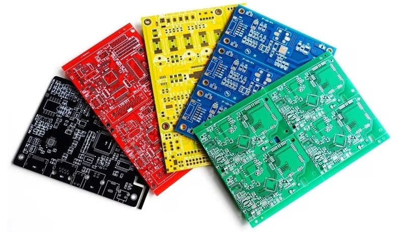
The green solder mask is applied over PCB copper traces to both prevent oxidation and avoid solder bridges during assembly. PCBs acquire their recognizable look through this protective layer. Afterward the silkscreen layer produces component identifiers and additional markings including labels directly on the board for assembly testing.
6.Surface Finishing
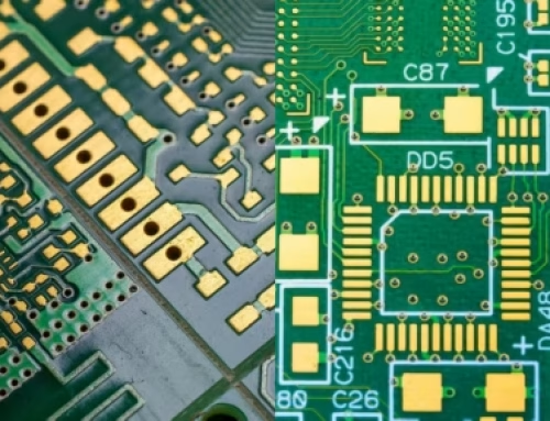
Common surface finishes used in PCBs include Electroless Nickel Immersion Gold (ENIG), Hot Air Solder Leveling (HASL), and Organic Solderability Preservative (OSP). Specific finishes give distinct benefits when employed rightly, including better solderability as well as better resistance to corrosion.
7.Electrical Testing and Quality Control
The board is subjected to comprehensive testing to verify its functionality before it moves to the assembly stage. Automated test systems detect open circuits and short circuits alongside other types of defects. Automated Optical Inspection (AOI) and Flying Probe Testing are two main methods used by PCB fabrication manufacturers to verify board integrity
Challenges and Innovations in PCB Fabrication

PCB Board Fabrication
The production of printed circuit boards experiences difficulties in achieving miniaturization along with maintaining high-frequency performance standards while also meeting environmental sustainability criteria.
The trend toward smaller device sizes requires manufacturers to develop PCBs that have finer traces and smaller, which push fabrication technology to its boundaries. 5G and IoT materials require accurate impedance control in combination with reduced dielectric loss properties.
Leading manufacturers have developed the High Density Interconnect (HDI) technology in order to break the challenges of industry in terms of functional design that’s compact.
Selecting the Trusted PCB Fabrication Manufacturer
The significance of choosing a dependable PCB fabrication manufacturer is vital to insure the success in electronic design. It’s essential to estimate PCB companies according to their experience and their instruments, including ISO 9001 or IPC norms as well as attesting their capability to produce multilayer boards as well as high- frequency designs.
Top manufacturers deliver end-to-end services starting from design consultation all the way to final assembly to maintain a smooth workflow.
Communication is also key. When manufacturers deliver defined timelines and transparent pricing along with quick support responses they help save time and minimize mistakes. Top companies provide prototyping services which enable designers to evaluate and perfect their boards before launching full-scale production.
Last Words!
The process of manufacturing PCB boards requires complex engineering precision while utilizing advanced technological developments. Every phase between the original design concept and the completed assembled board demands meticulous attention and specialized knowledge.
Designers and engineers can develop reliable and innovative electronic solutions when they partner with an experienced the manufacturer to actualize their ideas.
The electronics industry’s progression depends on designers working together with manufacturers because their combined efforts will continue to develop new technologies through individual circuit boards.
Table of Contents
Get Your PCB Quote!

