PCB Assembly Process: Complete Step-by-Step Guide
In today's interconnected world, almost every electronic device, from the smartphone in your pocket to the complex medical equipment saving lives, relies on a crucial manufacturing stage: PCB assembly. This guide explains the PCB assembly process from design preparation to final testing, covering SMT, THT, inspection, quality control.
Get Your PCB Quote!
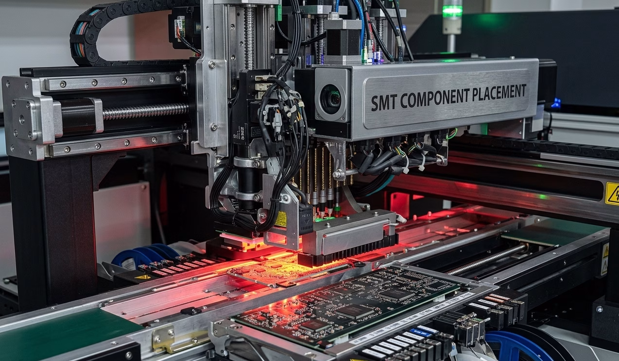
Table of Contents
- кіріспе
- ПХД құрастыру процесі дегеніміз не?
- Алдын ала құрастыру: Дизайнды тексеру (DFM/DFA)
- 1-қадам: дәнекерлеу пастасын қолдану
- 2-қадам: SMT компоненттерін орналастыру
- 3-қадам: Қайта ағынмен дәнекерлеу
- 4-қадам: Автоматтандырылған оптикалық тексеру (AOI)
- 5-қадам: Тесік арқылы бөлшекті құрастыру
- 6-қадам: Рентгендік тексеру (AXI)
- 7-қадам: Тізбек ішіндегі тестілеу (АКТ)
- 8-қадам: Функционалдық тестілеу
- 9-қадам: Тазалау және конформды жабынмен жабу
- 10-қадам: Соңғы сапаны бақылау және қаптама
- Баспа платасын жинау процесі: толық ағынға шолу
- SMT vs. Тесік арқылы: Дұрыс технологияны таңдау
- ПХД құрастырудағы жиі кездесетін ақаулар және оларды шешу жолдары
- ПХД құрастыруға арналған IPC стандарттары
- ПХД құрастыру шығындарын түсіну
- PCB жинау процесін сәтті аяқтауға арналған кеңестер
- Жиі Қойылатын Сұрақтар
- қысқаша мазмұндама
Introduction
This comprehensive guide breaks down every stage of the PCB assembly process—from design verification to final packaging—giving you the knowledge to work more effectively with your assembly partner or optimize your in-house operations. Whether you are launching your first prototype or scaling to high-volume production, understanding PCBA helps you make better design decisions, catch potential issues early, and build more reliable products.
What Is the PCB Assembly Process?
The PCB assembly process (often abbreviated as PCBA) transforms a bare printed circuit board into a functional electronic assembly by mounting and soldering components onto it. The bare PCB is like an empty city: the infrastructure exists, but nothing works until you add components. The process encompasses two main technologies:
- Surface Mount Technology (SMT): Components are placed directly onto the board surface and soldered in a reflow oven. This is the dominant method for modern electronics.
- Through-Hole Technology (THT): Component leads pass through drilled holes in the board and are soldered on the opposite side, providing superior mechanical strength for connectors and high-power parts.
Most modern assemblies combine both—SMT for the bulk of components, THT reserved for items requiring mechanical robustness or higher power handling.
| Assembly Type | Best For | Speed | Component Size |
| SMT | High-density designs, miniaturization | Fastest | 0201 packages and up |
| Through-Hole | Power components, connectors, mechanical stress | Moderate | Larger components |
| Mixed | Most production boards | Varies | Both types |
Pre-Assembly: Design Verification (DFM/DFA)
Before any components touch your board, assembly effectively begins with design verification. This step alone can save thousands of dollars and weeks of delays.
Design for Manufacturability (DFM) Check
A DFM check examines your PCB layout against the manufacturer’s fabrication capabilities, catching manufacturing problems while they are still cheap to fix—during design, not production. Key verification points include:
- Trace width and spacing: Minimum dimensions your fab house can reliably produce
- Drill sizes and aspect ratios: Ensuring holes can be properly plated
- Annular ring requirements: Adequate copper around drilled holes
- Solder mask clearances: Proper dam widths between pads
- Copper balance: Preventing board warpage during thermal stress
Design for Assembly (DFA) Check
DFA focuses on whether the board can be efficiently assembled. This includes verifying:
- Component footprint accuracy: Matching pads to actual component dimensions
- Component spacing: Adequate clearance for pick-and-place equipment
- Orientation markings: Clear polarity indicators for diodes, ICs, and electrolytic capacitors
- Fiducial markers: Reference points for automated placement equipment
- Panel optimization: Efficient use of production panels
| Check | Focus Area | Checks For |
| DFM | Fabrication | Trace width, drill sizes, clearances, copper weight |
| DFA | Assembly | Component placement, pad design, pick-and-place compatibility |
Bill of Materials (BOM) Verification
Your BOM is the shopping list for the entire assembly. Verification ensures part numbers match actual components, quantities are accurate, footprints correspond to specified packages, and alternatives are identified for supply-constrained parts. A single footprint mismatch—say, a 0603 capacitor footprint specified for an 0402 part—can delay a production run by days. Catching it in DFM takes minutes.
Need PCB Manufacturing or Assembly?
Get a free quote within 24 hours. We specialize in prototype-to-production PCB/PCBA for hardware teams worldwide.
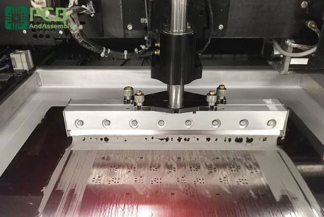
Step 1: Solder Paste Application
PCB assembly for SMT components begins with solder paste application. This gray, putty-like substance is a carefully formulated mixture of tiny solder spheres—typically 25–45 microns in diameter—suspended in flux. The flux activates during heating to remove surface oxides and promote proper wetting between solder and component leads.
The Stencil Printing Process
A precision-cut stainless steel stencil is aligned over the bare PCB using fiducial markers. The stencil’s apertures correspond exactly to the SMT pads where components will land. The process works as follows:
- The PCB is secured in a printing fixture
- The stencil is aligned using fiducial markers on the board
- Solder paste is deposited onto the stencil
- A metal squeegee blade sweeps across, forcing paste through the apertures
- The stencil lifts away, leaving precisely deposited paste deposits on each pad
Stencil thickness (typically 0.12–0.15mm) and aperture size together determine paste volume. Too much paste causes bridging; too little causes insufficient joints. Modern paste printers automate squeegee pressure and speed for consistent deposition across the board.
Solder Paste Composition
Modern lead-free solder paste uses SAC305 alloy as the industry standard, meeting RoHS compliance requirements:
| Element | Percentage | Purpose |
| Tin (Sn) | 96.5% | Primary bonding material |
| Silver (Ag) | 3.0% | Improves wetting and joint strength |
| Copper (Cu) | 0.5% | Reduces copper dissolution from pads |
Solder Paste Inspection (SPI)
Quality-focused assembly houses perform automated SPI immediately after printing. Using laser profilometry or camera-based systems, SPI measures:
- Paste volume on each pad: Ensuring adequate solder for reliable joint formation
- Paste height consistency: Detecting variations that indicate stencil wear or clogging
- Registration accuracy: Verifying paste is centered on pads, not shifted
- Bridging and insufficient deposits: Catching defects before components are placed
Catching paste defects at this stage is far more cost-effective than finding the resulting soldering failures after reflow—components are not yet committed, and no rework is required.
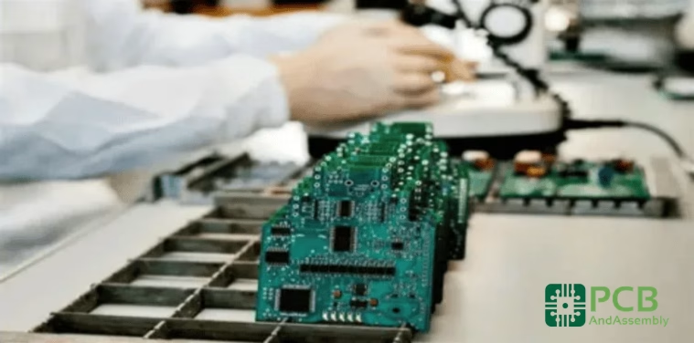
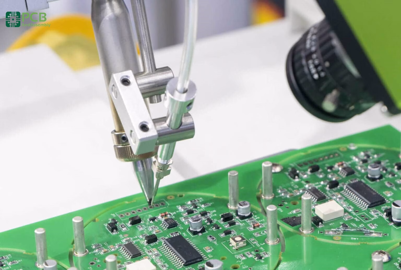
Step 2: SMT Component Placement
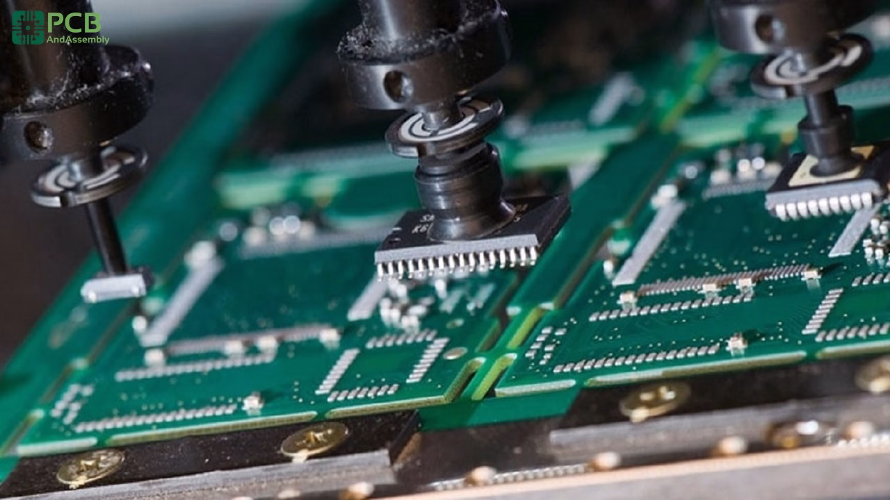
With solder paste applied, the board moves to pick-and-place machines—the workhorses of modern electronics assembly. These are high-precision robotic systems capable of placing thousands of components per hour with micron-level accuracy.
How Pick-and-Place Works
A modern pick-and-place system follows this sequence for every component:
- Picks a component from its feeder (reel, tray, or tube) using a vacuum nozzle
- Centers the component using optical alignment—a downward camera reads the component body
- Rotates the component to the correct orientation
- Places it on the designated pad location at speeds exceeding 100,000 placements per hour
The placement program is generated from your centroid file (also called XY data or pick-and-place file), which specifies each component’s X/Y coordinates, rotation angle, and reference designator. Modern equipment achieves placement accuracy of ±25–50 microns, essential for fine-pitch parts like 0.4mm BGAs or 0201 passives. The solder paste’s tackiness temporarily holds components in place until reflow creates permanent connections.
Component Feeding Methods
| Feed Type | Best For | Typical Components |
| Tape and Reel | High-volume, small components | Resistors, capacitors, small ICs |
| Tray | Larger or moisture-sensitive parts | BGAs, QFPs, large connectors |
| Tube | Medium quantities, IC packages | DIP packages, some connectors |
| Loose/Bowl | Special handling requirements | Odd-form components |
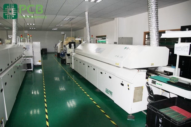
Step 3: Reflow Soldering
Reflow soldering transforms the assembly from a collection of loosely held components into a permanently bonded board. A poor reflow profile can damage components, create unreliable joints, or generate a board full of defects—getting it right is critical.
Understanding the Reflow Oven
Modern reflow ovens use forced-air convection heating with multiple independently controlled zones. Boards travel through on a conveyor, experiencing a precisely choreographed temperature journey. High-end production ovens feature 8–12 zones, allowing fine control over the thermal profile. The oven’s atmosphere also matters: nitrogen purging displaces oxygen, reducing oxidation of solder and component leads and improving wetting—particularly important for BGA assemblies.
The Reflow Temperature Profile
Every board requires a carefully optimized profile based on its thermal mass, component mix, and solder paste specification. The profile consists of four distinct zones:
- Preheat Zone (25°C → 150°C): Ramp rate 1–3°C/sec over 60–90 seconds. Gradually raises board temperature to activate flux and prevent thermal shock to sensitive components.
- Thermal Soak Zone (150°C → 200°C): Held for 60–120 seconds. Activates flux chemistry, drives off volatiles from the paste, and equalizes temperature across the board—critical for reducing Delta T between small passive components and large heat-sink packages.
- Reflow Zone (Peak: 235–250°C for lead-free): Time above liquidus (TAL) is 30–60 seconds. Solder melts and wets component leads and pads. Peak temperature is typically 20–40°C above the solder’s liquidus point. Exceeding the maximum exposure time risks component damage and intermetallic growth.
- Cooling Zone (250°C → ambient): Ramp rate 2–4°C/sec. Controlled cooling solidifies joints with the correct grain structure, ensuring reliability. Quenching too fast causes thermal shock; cooling too slowly produces coarse grain structure.
| Zone | Temperature Range | Duration | Key Parameter |
| Preheat | 25°C → 150°C | 60–90 sec | Ramp rate: 1–3°C/sec |
| Soak | 150°C → 200°C | 60–120 sec | Flux activation, Delta T reduction |
| Reflow | Peak 235–250°C | 30–60 sec TAL | Peak temp 20–40°C above liquidus |
| Cooling | 250°C → ambient | Controlled | Ramp rate: 2–4°C/sec |
Step 4: Automated Optical Inspection (AOI)
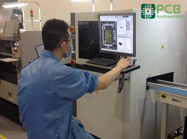
After reflow, the assembly passes through its first major quality gate. AOI machines use high-resolution multi-angle cameras and sophisticated image processing algorithms to scan the entire board surface.
What AOI Detects
- Missing components: Empty pads where components should be present
- Incorrect component: Wrong part placed at a location (verified against reference database)
- Orientation errors: Reversed polarity, rotated ICs or electrolytic capacitors
- Solder defects: Bridges between pads, insufficient solder, tombstoning of passive components
- Lifted leads: Component leads not properly seated on pads
- Wrong component values: Detectable via visible date codes or markings within optical limits
AOI Capabilities and Limitations
AOI excels at catching surface-level defects rapidly and non-destructively. However, it has a fundamental limitation: it cannot see hidden connections. This matters specifically for:
- BGA packages: Solder balls are hidden entirely beneath the component body
- QFN ground pads: Central thermal pad is inaccessible from above
- Internal PCB defects: Delamination, buried via failures, inner-layer opens
For all of the above, X-ray inspection (Step 6) is the only non-destructive solution.

Step 5: Through-Hole Component Assembly
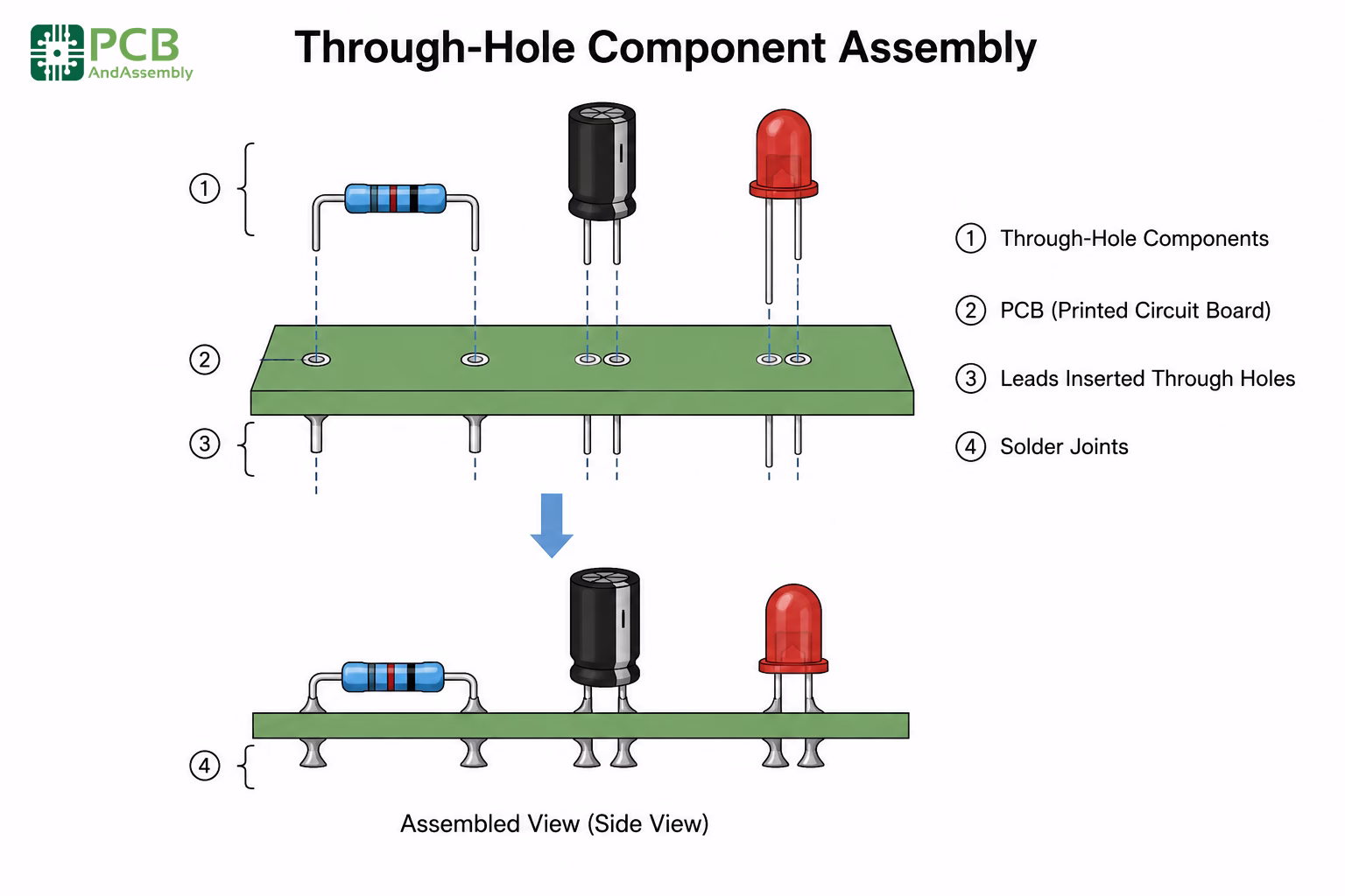
Many boards combine SMT with through-hole components—large connectors, electrolytic capacitors, power inductors, and any part that requires mechanical robustness. After SMT assembly and AOI sign-off, through-hole parts are inserted and soldered.
Through-Hole Insertion Methods
Manual Insertion
Used for low volumes, prototypes, or components that are unsuitable for automation. Operators insert components following assembly drawings and reference designator callouts, typically working at anti-static workstations with:
- Component sequence guides to enforce correct placement order
- Anti-static mats, wrist straps, and ESD-safe trays
- Insertion tools for tight board areas or long-lead components
Automated Insertion
High-volume production uses dedicated automated insertion equipment for standard THT packages:
- Axial insertion machines: For axial-leaded resistors and diodes—components are cut, formed, and inserted in one motion
- Radial insertion machines: For radial electrolytic capacitors and other radial-lead components
- DIP insertion machines: For dual in-line IC packages, sockets, and similar through-hole ICs
Wave Soldering
Wave soldering is the traditional mass-soldering method for through-hole boards. The process runs in four stages:
- Flux application: Spray or foam flux coats the bottom side of the PCB, cleaning pad and lead surfaces in preparation for solder contact
- Preheating: Board temperature rises to 100–150°C, activating the flux and preventing thermal shock when the board contacts molten solder
- Wave contact: The board passes over a standing wave of molten solder at 250–260°C (lead-free). Solder wets the leads and through-hole pads, forming fillets as the board exits the wave
- Cooling: Controlled cool-down solidifies joints
Wave soldering works well for pure through-hole boards or boards with SMT components only on the top side. It struggles with double-sided SMT assemblies because bottom-side components would be submerged directly in molten solder—which is where selective soldering comes in.
Selective Soldering
For mixed-technology assemblies with SMT components on both sides, selective soldering targets only the through-hole locations without exposing bottom-side SMT components to a full solder bath:
- A programmable solder nozzle—or mini-wave—applies solder to specific pad locations only
- Bottom-side SMT components remain fully protected throughout the process
- Individual process parameters (temperature, dwell time, solder flow rate) can be set per joint
- Flux is applied locally rather than to the whole board
Selective soldering is slower than wave soldering but provides essential precision for complex mixed-technology assemblies.
| Soldering Method | Best For | Throughput | Precision |
| Wave Soldering | High-volume THT, single-sided boards | Highest | Moderate |
| Selective Soldering | Mixed technology, double-sided boards | Moderate | High |
| Manual Soldering | Low volume, rework, specialized joints | Lowest | Operator-dependent |
Step 6: X-Ray Inspection (AXI)
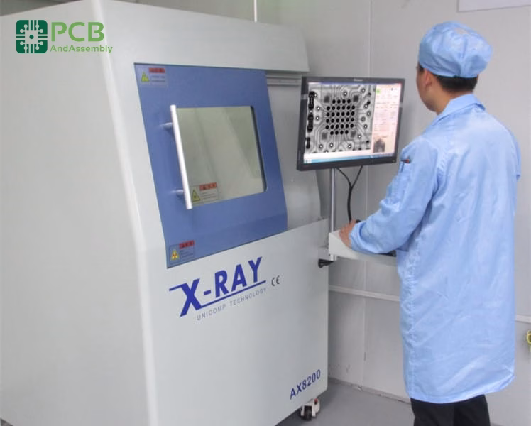
When a solder joint cannot be seen from the surface, you need to look through it. Automated X-ray Inspection is the standard solution for verifying hidden connections non-destructively.
When X-Ray Is Required
- BGA packages: Verifying all solder ball connections—potentially hundreds of them—beneath the component body
- QFN and QFP packages: Inspecting the central thermal/ground pad that is entirely hidden
- PTH hole fill: Confirming adequate solder penetration through plated through-holes (IPC-A-610 requires minimum 75% fill)
- Voiding analysis: Measuring void percentage in solder joints, particularly under power components where voids increase thermal resistance
What X-Ray Reveals
- Solder voids: Gas pockets trapped in the joint that reduce mechanical strength and thermal conductivity
- Head-in-pillow defects: Incomplete fusion of BGA solder balls, often caused by package warpage during reflow or surface oxidation
- Bridging under components: Solder shorts between adjacent BGA balls or QFN pads that are invisible from the surface
- Cold joints and insufficient wetting: Poor solder coverage indicating reflow profile problems or contaminated surfaces
Modern 3D AXI (computed tomography) adds the ability to slice through the board layer by layer, enabling complete inspection of multilayer assemblies without any destructive cross-sectioning.
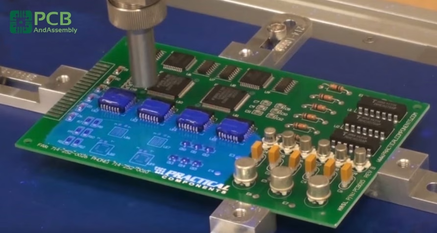
Step 7: In-Circuit Testing (ICT)
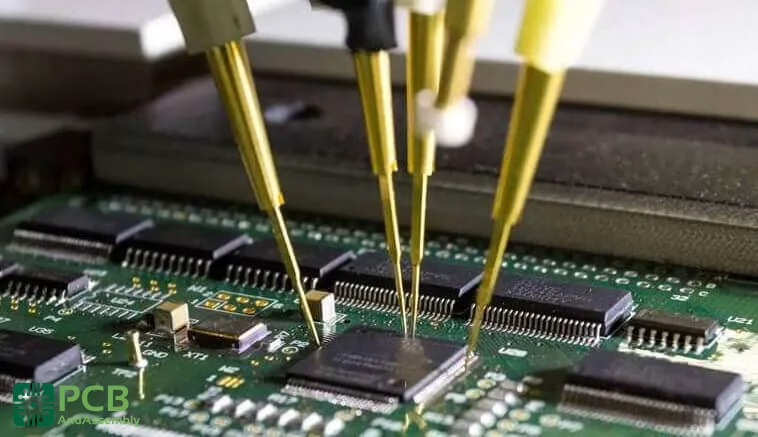
ICT provides comprehensive electrical verification that every component is present, correctly oriented, and within specification. It is the primary tool for catching manufacturing defects before functional testing.
How ICT Works
The assembled board is placed on a bed-of-nails fixture—a custom test jig with spring-loaded probes that simultaneously contact all designated test points on the PCB. In a single test cycle, ICT verifies:
- Component presence: Open-circuit detection for missing parts
- Correct values: Resistance, capacitance, and inductance measurements against design tolerances
- Shorts detection: Finding unintended connections between nets
- Diode and transistor polarity: Verifying orientation of polarized semiconductor devices
- IC pin connectivity: Confirming proper seating and contact for packaged ICs
ICT vs. Flying Probe Testing
Flying probe testers use movable probes instead of a fixed fixture, trading test speed for flexibility. This makes them ideal for prototypes and low-to-medium volumes where the cost of a custom bed-of-nails fixture cannot be justified.
| Test Method | Setup Cost | Test Speed | Best For |
| Bed-of-Nails ICT | High (custom fixture per board) | Very fast (parallel probing) | High-volume production |
| Flying Probe | Low (programming only) | Slower (sequential probing) | Prototypes, low-medium volume |
Step 8: Functional Testing
Where ICT verifies that individual components are present and correctly valued, functional testing confirms the assembled board actually performs as designed. It is the final electrical quality gate before packaging.
Functional Test Scope
Depending on the product, functional testing may encompass:
- Power-on testing: Verifying all power supply rails come up correctly and current consumption is within specification
- Signal integrity: Checking waveforms, timing margins, and signal levels at key test nodes
- Communication verification: Testing serial buses (I2C, SPI, UART), USB, Ethernet, and wireless links
- Sensor calibration: Programming initial calibration values for sensors, ADCs, and other precision components
- Firmware loading: Installing initial software and verifying boot behavior
- Full system simulation: Testing the board in its intended operating environment against complete functional requirements
Test Coverage Strategy
A robust test strategy layers multiple methods to catch different defect types:
- AOI: Catches visual and placement defects immediately post-reflow
- X-ray: Inspects hidden solder connections that optics cannot reach
- ICT: Verifies electrical connectivity and component values across the whole board
- Functional test: Confirms the design works as intended in operation
Each layer covers the gaps of the previous one. Together they provide comprehensive quality assurance from the very first placement through final sign-off.
Step 9: Cleaning and Conformal Coating
Depending on the product’s end-use environment and flux chemistry used in assembly, post-solder processing includes cleaning and, where needed, protective conformal coating.
PCB Cleaning
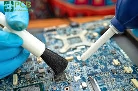
Flux residues left on the board after soldering can cause corrosion, electrochemical migration, and long-term reliability failures if not addressed. The appropriate cleaning approach depends on the flux type used:
- No-clean flux: Engineered to leave low-activity, benign residues—acceptable without cleaning in most applications. Cannot be cleaned with water alone if cleaning becomes required later.
- Water-soluble flux: Highly active chemistry that produces excellent solder wetting, but residues are ionic and must be removed with deionized water washing.
- Rosin flux: Traditional chemistry requiring solvent or aqueous-saponifier cleaning.
Common cleaning methods include batch spray washers, inline conveyorized washers for high-volume production, and ultrasonic cleaning tanks for boards with tight component spacing.
Conformal Coating
For products deployed in harsh environments, a thin conformal coating is applied to the finished assembly to protect against moisture, dust, chemical exposure, and temperature extremes.
| Coating Type | Protection Level | Typical Applications |
| Acrylic | Moderate; easy to rework | Consumer electronics, general use |
| Silicone | Good thermal and humidity range | Automotive, LED lighting |
| Polyurethane | Excellent chemical resistance | Industrial, military |
| Epoxy | Maximum protection; difficult to rework | Aerospace, harsh environments |
Application methods include selective spray (robotic nozzle deposits coating only on designated areas, masking connectors and test points), dip coating (full board immersion for complete coverage), and brush application for touch-up or low-volume work.
Step 10: Final Quality Control and Packaging
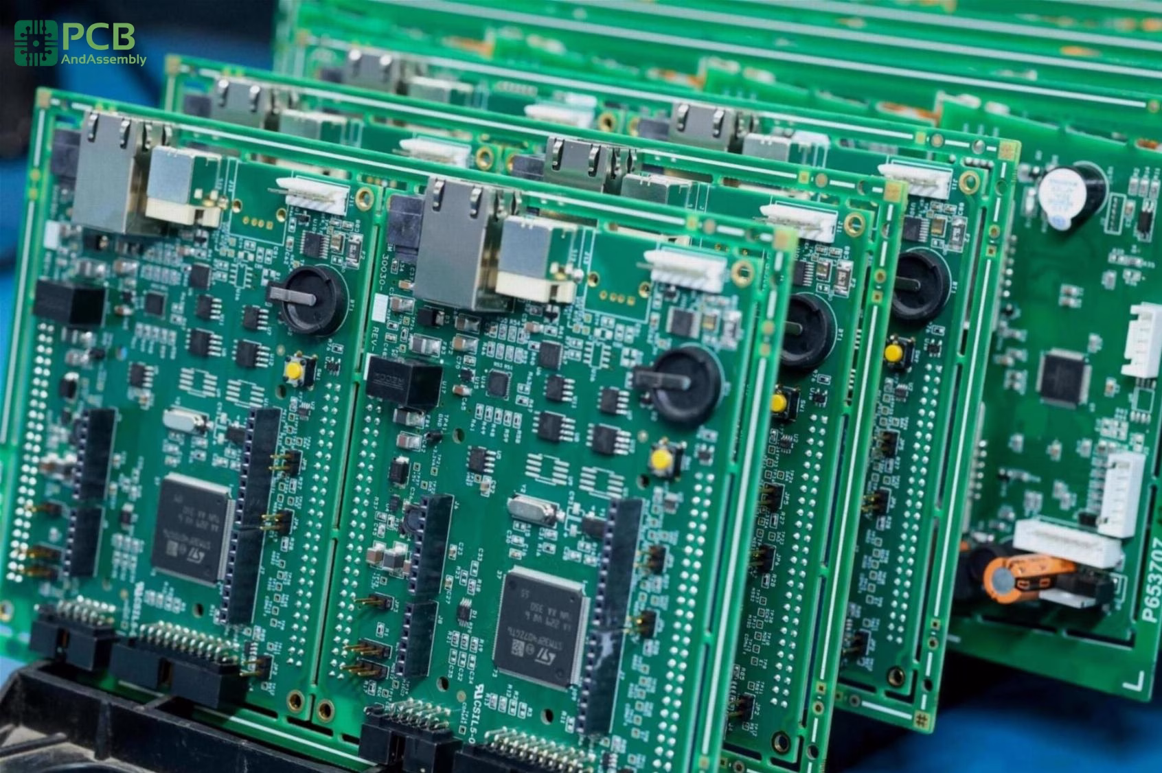
The final station combines comprehensive quality sign-off with preparation for safe shipment. No board leaves the facility without passing both.
Final QC Inspection
- Visual workmanship inspection: Human or automated review against IPC-A-610 acceptance criteria for the applicable product class
- Part marking and label verification: Confirming correct date codes, lot codes, and assembly revision labels are applied
- Dimensional checks: Verifying connector positions, board outline, and any mechanical tolerances specified in drawings
- Documentation verification: Confirming test records, certificates of conformance, and traceability records are complete and match the shipment
ESD-Safe Packaging
Electronic assemblies are sensitive to electrostatic discharge throughout their lifecycle—a single ESD event during packaging or transit can destroy a device that passed all tests. Proper packaging includes:
- Anti-static bags: Pink poly bags for general protection, or metalized shielding bags for assemblies requiring Faraday cage shielding
- Moisture barrier bags with desiccant: For moisture-sensitive assemblies (IPC/JEDEC J-STD-033 MSL ratings), sealed bags with desiccant and humidity indicators
- Labeling and traceability: Date codes, lot numbers, revision levels, and ESD warning symbols on all packaging
- Cushioning and cartonization: Foam inserts, anti-static foam, and corrugated cartons appropriate for the shipment’s transport method
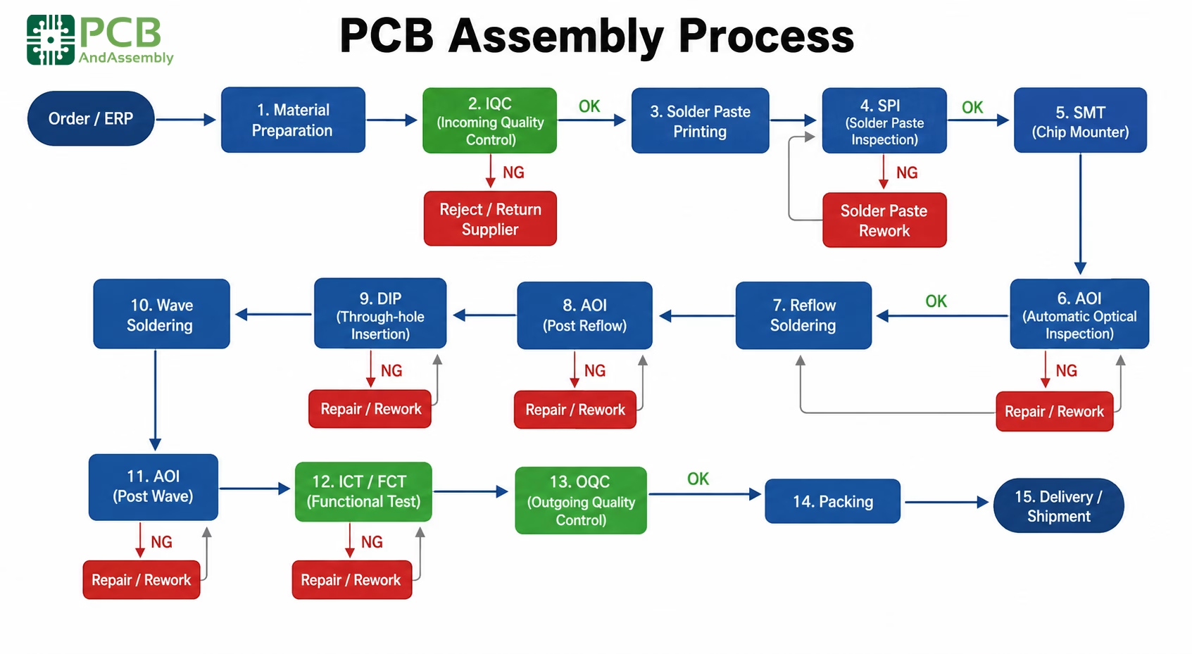
PCB Assembly Process: Complete Flow at a Glance
| Step | Process | Key Purpose |
| 0 | DFM/DFA Check | Prevent manufacturing issues before production begins |
| 1 | Solder Paste Application | Deposit precise solder deposits on SMT pads via stencil |
| 2 | SMT Component Placement | Position all surface-mount components with pick-and-place |
| 3 | Reflow Soldering | Permanently bond SMT components through controlled heating |
| 4 | AOI Inspection | Detect all surface-level placement and solder defects |
| 5 | Through-Hole Assembly | Insert THT components and solder via wave or selective methods |
| 6 | X-Ray Inspection (AXI) | Inspect hidden connections (BGAs, QFNs, PTH fill) |
| 7 | In-Circuit Testing (ICT) | Verify electrical connectivity and component values |
| 8 | Functional Testing | Confirm full operational performance against spec |
| 9 | Cleaning and Conformal Coating | Remove flux residues and apply environmental protection |
| 10 | Final QC and Packaging | Quality sign-off, traceability, and ESD-safe shipment |
SMT vs. Through-Hole: Choosing the Right Technology
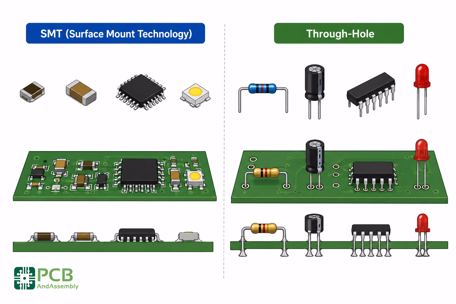
When to Choose SMT
- Size and density: A 0402 resistor measures just 1.0mm × 0.5mm—you could fit dozens where one through-hole resistor would go. SMT components can also be placed on both sides of the board, effectively doubling usable real estate.
- Speed and automation: Pick-and-place at 100,000+ components per hour followed by a single reflow pass makes SMT dramatically faster than any THT alternative.
- Cost at volume: Automation efficiency and smaller board sizes reduce per-unit cost significantly at production quantities.
When Through-Hole Still Makes Sense
- High mechanical stress: Connectors that get plugged and unplugged repeatedly need the physical anchor of leads extending through the board. The joint resists pull-out forces that would tear surface-mount pads away.
- High power components: Power resistors, large capacitors, and transformers benefit from through-hole mounting for improved thermal dissipation and mechanical stability.
- Field serviceability: Through-hole components are significantly easier to rework with basic soldering equipment—important for products serviced in the field.
- Availability: Some specialty components simply have no surface-mount equivalent.
| Feature | SMT | THT |
| Component Size | Smaller, lighter | Larger, heavier |
| Board Density | High (both sides of board) | Lower (typically one side) |
| Automation | Highly automated | Often manual or semi-automated |
| Mechanical Strength | Lower (relies on solder tension) | Higher (leads pass through board) |
| Assembly Cost | Generally lower at volume | Higher per placement |
| Best Applications | Consumer electronics, high-frequency circuits | High-power, connectors, mechanical stress |
Common PCB Assembly Defects and Solutions
| Defect | Cause | Prevention |
| Solder bridging | Excessive paste volume, tight component pitch | Proper stencil aperture design, adequate pad spacing |
| Tombstoning | Uneven pad heating, pad size imbalance | Thermal symmetry in layout, correct component orientation |
| Cold solder joint | Insufficient heat, board/component contamination | Optimized reflow profile, clean storage and handling |
| Voiding | Trapped flux gases, moisture in paste or PCB | Profile optimization, correct paste storage, pre-baking |
| Head-in-pillow | BGA package warpage during reflow, surface oxidation | Nitrogen atmosphere reflow, pre-bake BGAs before assembly |
| Missing components | Feeder jam, vacuum nozzle failure, empty reel | Automated feeder monitoring, post-placement vision check |
IPC Standards for PCB Assembly
| Standard | Scope |
| IPC-A-610 | Acceptability of Electronic Assemblies—the primary visual acceptance standard |
| IPC J-STD-001 | Requirements for Soldered Electrical and Electronic Assemblies |
| IPC-7711/7721 | Rework, Modification, and Repair of Electronic Assemblies |
| IPC-A-600 | Acceptability of Printed Boards (bare board quality) |
| IPC-2221 | Generic Standard on Printed Board Design |
IPC Product Classes
- Class 1: General Electronics: Consumer products where cosmetic imperfections are acceptable as long as function is maintained.
- Class 2: Dedicated Service Electronics: Communication equipment and industrial controls where extended life and reliable performance are expected.
- Class 3: High Reliability Electronics: Aerospace, medical, and military applications where failure is not acceptable and equipment must perform on demand.
Understanding PCB Assembly Costs
Understanding cost drivers helps you optimize both design and purchasing decisions.
Key Cost Factors
- Component count: More components mean more placement operations. Consolidate values where possible without sacrificing functionality.
- Component types: Standard SMT passives are cheapest to place. BGAs, fine-pitch QFPs, and 0201/01005 packages require more precision and cost more. THT adds wave or selective soldering steps.
- Board complexity: Double-sided assembly, high layer counts, tight tolerances, and special surface finishes all add cost.
- Quantity: Setup costs (programming, stencils, custom fixtures) are amortized over volume. A 10-piece prototype run has dramatically higher per-unit cost than a 10,000-piece production run.
- Turnaround time: Quick-turn services command a meaningful premium. Standard lead times are more economical when schedule allows.
Assembly Models
| Assembly Model | Your Responsibility | Cost Level | Best For |
| Full Turnkey | Documentation only | Highest | Convenience, low volume, first articles |
| Partial Turnkey | Long-lead and specialty parts only | Medium | Cost optimization with supply chain control |
| Consigned | All components and bare boards | Lowest | High volume, tightly controlled supply chain |
About PCBAndAssembly
Time is money in your projects – and PCBAndAssembly gets it. PCBAndAssembly is a PCB assembly company that delivers fast, flawless results every time. Our comprehensive PCB assembly services include expert engineering support at every step, ensuring top quality in every board. As a leading PCB assembly manufacturer, we provide a one-stop solution that streamlines your supply chain. Partner with our advanced PCB prototype factory for quick turnarounds and superior results you can trust.
Tips for a Successful PCB Assembly Process
Design Phase
- Engage your assembler early: Their DFM feedback during design prevents redesign cycles. Don’t wait until the layout is complete.
- Use standard footprints: Follow manufacturer-recommended land patterns or IPC-7351 standards. Custom footprints are a leading source of assembly problems.
- Consolidate component values: Standardizing on common values (10K resistors, 100nF capacitors) reduces BOM cost and supply chain risk.
- Include test points from the start: Adding test access after layout is far harder than designing it in initially.
- Mind thermal relief: Components on large copper pours need thermal relief patterns to prevent acting as heat sinks during soldering, which causes cold joints.
Documentation
- Use manufacturer part numbers (MPNs): ’10K 0603 resistor’ leaves room for interpretation—a specific MPN does not.
- Mark polarity on assembly drawings: Every polarized component should have its orientation clearly called out.
- Version-control everything: Revision numbers and dates on all files prevent the mismatched-document confusion that is a common cause of assembly errors.
Working with Your Assembly Partner
- Review the first article carefully: Before committing to a production run, inspect a first-article sample thoroughly. Issues caught here are not multiplied.
- Communicate changes formally: Any design change—even minor ones—requires updated documentation with a new revision number.
- Confirm component availability early: Component lead times have become highly variable. Always verify stock before committing to a production schedule.
Frequently Asked Questions
What is the difference between PCB and PCBA?
A PCB (Printed Circuit Board) is the bare board—copper traces, vias, and pads on a substrate, but no components. PCBA (Printed Circuit Board Assembly) is the same board after all components have been mounted and soldered, making it a functional electronic assembly ready for integration into an end product.
How long does PCB assembly typically take?
- Prototype / quick-turn: 24 hours to 5 days for small quantities with components in stock
- Standard production: 1–3 weeks for medium volumes
- High-volume with component procurement: 4–8 weeks when the assembly house is sourcing parts
Turnkey services typically add 1–2 weeks for component sourcing. Always confirm component availability before committing to a schedule—lead times for some parts remain highly variable.
What files are needed for PCB assembly?
Minimum requirements: Gerber files (copper layers, solder mask, silkscreen, drill files), Bill of Materials with manufacturer part numbers and reference designators, centroid/XY file with placement coordinates and rotation angles, and an assembly drawing with orientation callouts and special instructions. Providing schematics, native CAD files (Altium, KiCad, Eagle), and test documentation significantly reduces the chance of questions and delays. Many assembly houses also accept ODB++ or IPC-2581 formats, which bundle all necessary data into a single intelligent package.
Can SMT and THT components be used on the same board?
Yes—mixed technology is the norm for most production boards. SMT handles the majority of components for density and automation efficiency, while THT is used for connectors, high-power components, and parts requiring mechanical robustness. Selective soldering allows both technologies to coexist on double-sided boards without compromising either.
What are the most common PCB assembly defects?
The most frequently encountered defects are solder bridges (unintended shorts between pads), opens (missing or incomplete solder joints), tombstoning of passive components (one end lifts due to uneven heating), cold joints, voids in BGA solder balls, head-in-pillow on BGAs, and missing or misoriented components. Most can be traced back to paste deposition, reflow profile, or component placement issues—all controllable through proper process setup and inspection.
How do I select the right assembly house?
Evaluate on technical capabilities (can they handle your component types and tolerances?), relevant certifications (ISO 9001 baseline; AS9100, ISO 13485, or IATF 16949 if your industry requires it), volume fit (prototypes vs. high-volume production lines are fundamentally different businesses), inspection capabilities (AOI, X-ray, ICT, functional test), quality of DFM support, and references from customers with similar product requirements.
Summary
The PCB assembly process is a precisely orchestrated sequence of engineering steps that transforms a bare board into the functional heart of an electronic device. From rigorous design verification through solder paste deposition, automated component placement, reflow soldering, multi-stage optical and X-ray inspection, through-hole assembly, electrical testing, cleaning, conformal coating, and final quality control—every step serves a defined purpose and directly impacts the reliability of the finished product.
Understanding each stage makes you a better design partner, helps you communicate more effectively with your assembly house, and equips you to make informed decisions about design tradeoffs, inspection requirements, and test strategy. The investment in understanding the process always pays off in fewer surprises, faster production cycles, and more reliable products.

Get Quote Free