PCB Jumper Wires: What is it and How to Use Them
A PCB jumper is a small wire or conductive trace. It can be used to connect two or more locations on the board. It is employed to create a short circuit between different circuit components or to bypass a portion of the circuitry.
Get Your PCB Quote!
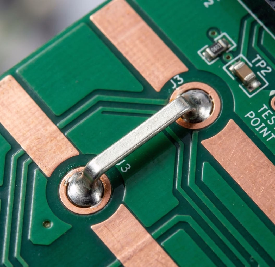
Table of Contents
1. Introduction
Jumper wires provide a flexible and often cost-effective way to navigate complex routing challenges that standard copper traces cannot easily overcome. Whether it’s to provide an alternative path when resources are limited, to allow for dynamic electrical connections, or to facilitate testing and configuration, jumpers are a versatile tool in any PCB designer’s arsenal. This article delves deep into the world of jumper wires, exploring their functions, various types, practical applications, and best practices for their effective integration into your circuit board designs.
2. What are Jumper Wires?
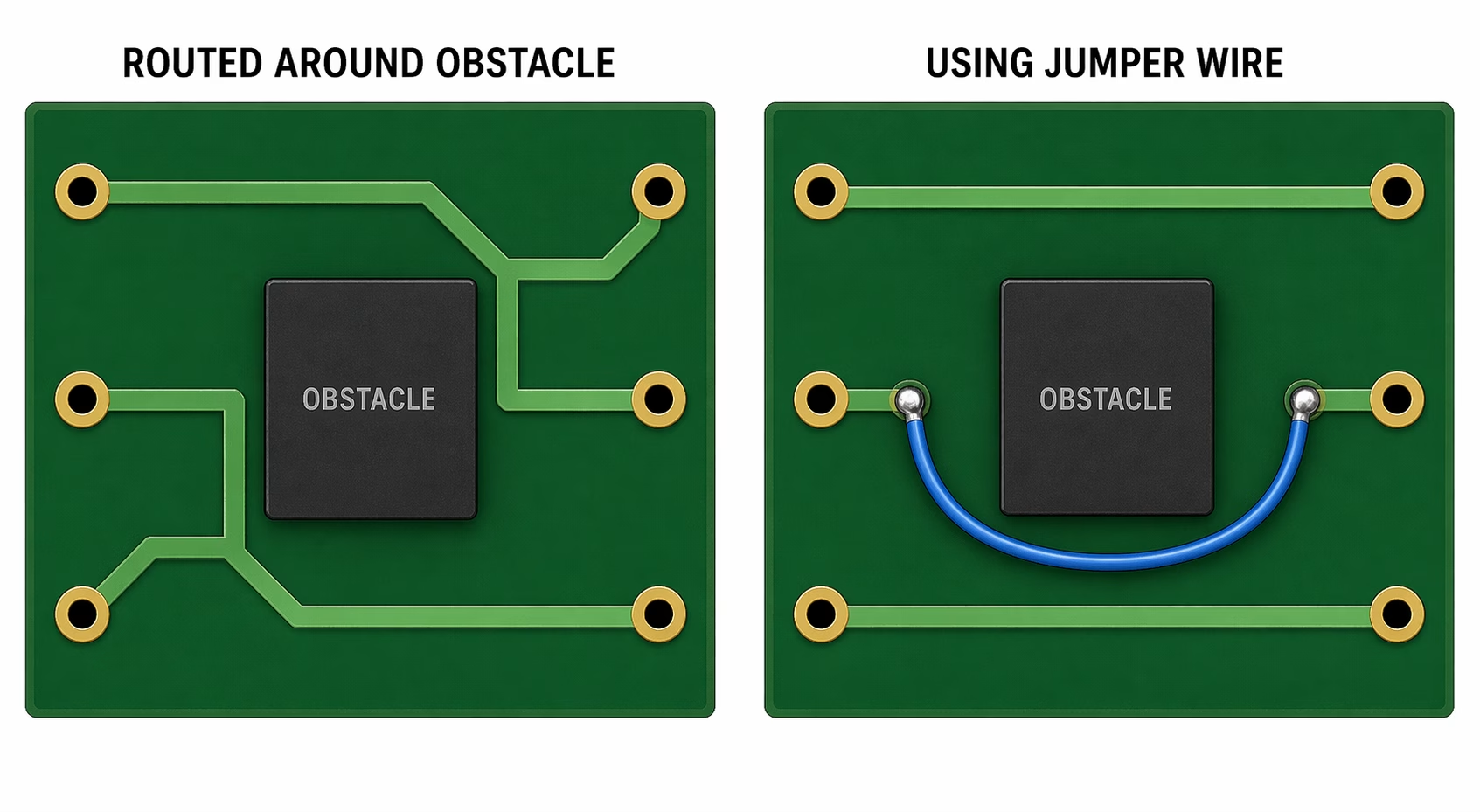
At its core, a jumper wire in PCB design is an electrical connection that bridges two or more points on a circuit board, bypassing the conventional copper traces. These connections can be either temporary or permanent, serving various strategic purposes within an electronic circuit. Unlike the etched pathways on a PCB, jumpers are typically discrete components or manual additions designed to establish a link where direct trace routing is impractical or impossible due to layout constraints.
The primary functions of a jumper wire extend beyond mere connectivity:
- Enabling Complex Connections:When dense component placement or limited board layers prevent a direct copper trace connection, a jumper offers an essential alternative path. This is particularly relevant in single and double-layer PCBs where routing space is at a premium.
- Providing Alternative Routing Paths:Jumpers offer a ” plan B” for electrical connections, especially valuable when standard layout resources are exhausted or undesirable. They can help avoid complex via structures or multiple layers that would increase manufacturing cost and complexity.
- Signal Separation and Flexibility:Jumper wires can provide flexible electrical connections or isolation between different functional blocks of a circuit. This allows for easy modification of a circuit’s behavior without redesigning the entire board, facilitating different operating modes or configurations.
- Improving Reliability and Preventing Issues:By offering a dedicated path, jumpers can prevent signal degradation or manufacturing issues that might arise from forced, inefficient, or overly narrow trace routing. They can also act as sacrificial links in certain test scenarios.
- Facilitating Rework and Prototyping:During early design phases or post-production modifications, jumpers are invaluable. They allow engineers to quickly test different circuit variations, bypass faulty sections, or add missing connections without incurring the cost and time of a new PCB fabrication run. This makes them a go-to solution for rapid prototyping and iterative development.
Essentially, jumper wires are a problem-solving mechanism, ensuring that functionality is achieved even when ideal trace routing isn’t feasible. They demonstrate the ingenuity within circuit board design to overcome physical limitations with practical solutions.
3. Why Use Jumper Wires?
The decision to incorporate jumper wires into a PCB design is often driven by a combination of practical benefits, addressing both economic and engineering considerations. Their value becomes especially apparent in specific scenarios :
3.1. Cost-Sensitive Designs and Low-Layer Count PCBs
One of the most significant advantages of jumper wires is their role in reducing manufacturing costs. Multi-layer PCBs, with their sophisticated stack-up structures and complex via technologies, offer immense routing flexibility but come at a higher price point. For projects with strict budget constraints, particularly those utilizing single-layer or double-layer PCBs, jumper wires provide an elegant workaround for routing congestion . By strategically placing jumpers, designers can avoid adding extra layers, thereby cutting down on fabrication expenses. This makes them an indispensable tool in creating economical and efficient cost-sensitive designs.
3.2. Prototyping and Testing Flexibility
In the initial stages of product development, rapid prototyping is key. Jumper wires are a designer’s best friend for quickly iterating on a circuit. They allow engineers to:
- Test different circuit variations without committing to a full PCB re-spin.
- Temporarily enable or disable specific functionalities.
- Bypass sections of a circuit for fault isolation during debugging .
- Integrate late-stage modifications or add features post-layout.
This flexibility significantly accelerates the development cycle, saving both time and resources during the critical testing phase.
3.3. Post-Production Rework and Repairs
Even with meticulous design and manufacturing, unforeseen issues can arise. A trace might be incorrectly routed, a component might need a different connection, or a design flaw might be discovered after fabrication. In such cases, jumper wires offer a practical solution for rework and repair. Instead of scrapping an entire batch of PCBs, a technician can install a jumper wire to correct the connection, extending the life and usability of the board. This is particularly valuable for high-value or complex assemblies where replacement is not a viable option.
3.4. Configuration and Customization Options
Jumpers are also excellent for providing user-configurable settings or semi-permanent setup options. For instance, a single PCB design could serve multiple purposes by changing a jumper’s position, allowing for different operating modes, voltage selections, or input/output configurations. This enables greater product versatility from a standardized hardware platform, catering to diverse application requirements through simple physical changes. These configuration options are highly beneficial for end-users and manufacturers alike.
4. Types of Jumper Wire Implementations in PCB Design
While the concept of a jumper wire is simple, its implementation can take several forms, each suited to different design needs, manufacturing processes, and levels of permanence. Understanding these options allows designers to select the most appropriate solution for their specific PCB layout challenges.
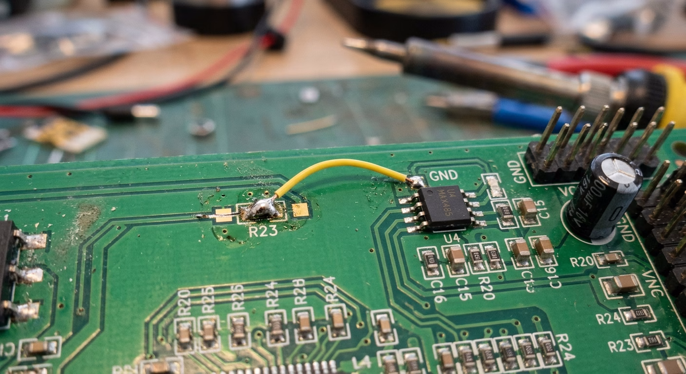
4.1. Manual Wire Jumpers
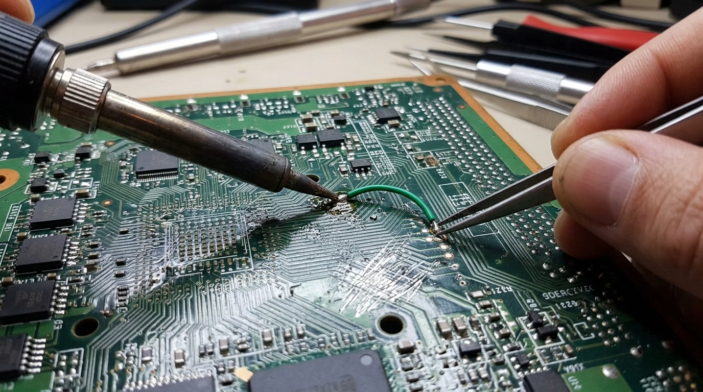
The simplest and most direct form of a jumper is a length of conductive wire, often insulated, manually soldered onto the PCB. These are typically used for:
- Quick fixes or modifications during prototyping.
- Bridging longer distances where other jumper types are less practical .
- Creating temporary connections for testing.
Wire jumpers are highly flexible but require manual installation, which can increase assembly time and introduces the potential for human error. They are a fundamental method of addressing an unexpected routing challenge.
4.2. Jumper Caps (Shunts) and Header Pins
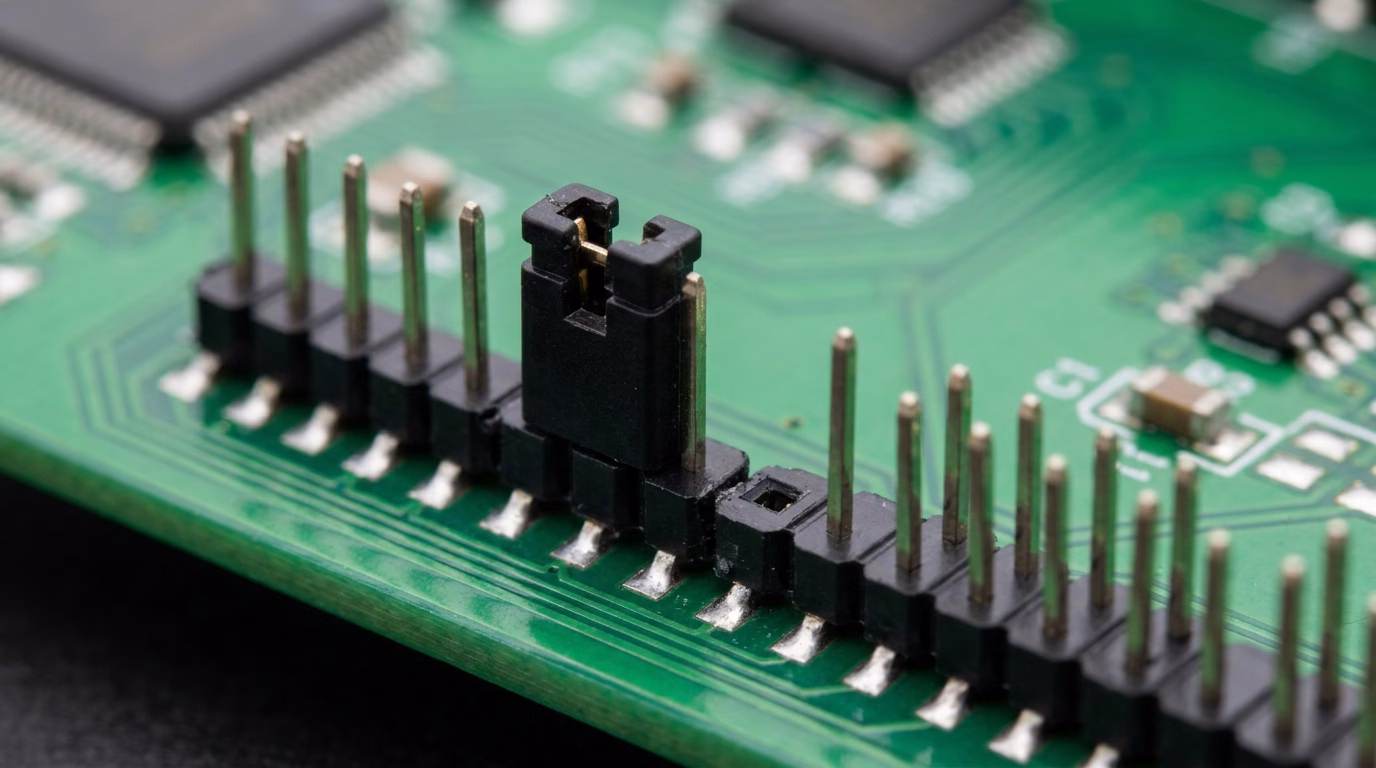
This common type involves a set of header pins (typically 2 or 3) soldered onto the PCB, over which a small conductive “jumper cap” or “shunt” can be placed. The cap short-circuits two adjacent pins, establishing a connection.
| Feature | Description | Application |
| Header Pins | Standard through-hole or surface-mount pins. | Permanent fixture on PCB for jumper connection. |
| Jumper Cap | Small plastic housing with internal metal clip . | Temporary or semi-permanent configuration changes. |
This method offers:
- Ease of modification by end-users or technicians without soldering.
- Clear visual indication of the connection status.
- Common use for selecting different modes, setting addresses, or enabling/disabling features (e.g., master/slave settings).
Jumper caps are ideal for configuration options that might need to be changed after manufacturing.
4.3. Zero-Ohm Resistors
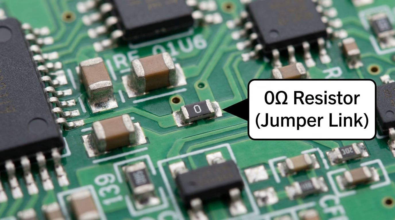
A zero-ohm resistor (also known as a “jumper resistor” ;) is an SMD (Surface Mount Device) component that looks like a standard resistor but has a nominal resistance of zero ohms. These components are used to:
- Bridge traces on a single layer, especially for crossing signals in an otherwise busy area.
- Allow for automatic placement during SMT assembly, reducing manual labor compared to wire jumpers.
- Maintain consistent component footprints on the BOM, making production easier if some connections are jumpers and others are actual resistors.
They are a cleaner, more professional-looking solution for permanent jumper connections in automated assembly environments. Using a zero-ohm resistor is a common practice in modern PCB manufacturing .
4.4. Solder Bridges
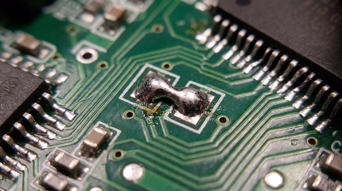
A solder bridge is created by simply placing two adjacent pads on the PCB and bridging them with a blob of solder. This is often referred to as a “no-B OM” (Bill of Materials) solution because it doesn’t require an additional component. Advantages include:
- Extremely low cost and minimal board space.
- Permanent connection once soldered.
- Useful for small, non-critical connections or late-stage design modifications where component space is limited.
The main drawback is that changing a solder bridge requires desoldering, which can be more difficult than removing a jumper cap. Despite this, it’s an efficient way to resolve minor routing challenges.
4.5. Programmable Jumpers (Less Common)
While not strictly “wire” jumpers, some advanced systems incorporate programmable jumpers. These might involve small, reconfigurable switches (like DIP switches) or even fuses/eFuses that can be programmed once or multiple times to establish connections. These are typically found in more complex , high-reliability systems where dynamic configuration or security features are paramount, offering a sophisticated form of configuration options.
5. Best Practices for Incorporating Jumper Wires
While jumper wires offer significant advantages, their implementation should be carefully considered to maintain signal integrity, ease of manufacturing, and overall board reliability. Adhering to best practices ensures that jumpers enhance, rather than compromise, your circuit board design.
5.1. Minimize Jumper Length and Number
As a general rule, try to keep jumper wires as short as possible. Longer wires can introduce parasitic inductance and capacitance, potentially affecting high-frequency signals or creating noise. Additionally, minimize the total number of jumpers on a board. Excessive jumpers can clutter the layout, complicate assembly, and increase the likelihood of errors during manual installation or rework.
5.2. Avoid Critical Signal Paths
Jumpers should ideally not be used for high-speed, high-frequency, or sensitive analog signals. The inherent non-uniformity and potential for interference make them unsuitable for paths where signal integrity is paramount. Reserve jumpers for static connections, power lines, or low-speed digital signals where minor impedance mismatches are less critical.
5.3. Plan for Manufacturing and Assembly
If using manual wire jumpers, consider the assembly process. Clearly indicate jumper locations on the silkscreen and in assembly documentation. For zero-ohm resistors, ensure they are compatible with automated pick-and-place machines. For jumper caps, ensure adequate clearance for easy installation and removal by hand. Thoughtful planning reduces errors and speeds up production, especially in cost-sensitive designs.
5.4. Document Jumper Functions Clearly
Thorough documentation is crucial . Label jumper locations and their functions clearly on the PCB silkscreen (e.g., “J1: Mode Select,” “JP2: 5V/3.3V”). Include a section in the product manual or design documentation explaining how to configure jumpers, especially if they provide configuration options for the end-user. This prevents confusion during testing, debugging, and field deployment.
5.5. Prioritize Robustness for Permanent Connections
For permanent connections, solder bridges or zero-ohm resistors are generally more robust than manual wire jumpers. If wire jumpers are unavoidable, ensure they are securely soldered and, if necessary, anchored to prevent stress on solder joints from vibration or handling . Consider potting or conformal coating for added mechanical stability in harsh environments.
5.6. Use Jumpers as a Last Resort for Routing
While jumpers are a valuable tool for overcoming routing challenges, they should be considered a last resort for complex signal routing. Whenever possible, optimize your PCB layout to route all connections using copper traces, even if it requires careful component placement or slight adjustments to the board shape. Jumpers are best utilized for deliberate configuration or unavoidable constraints, not as a primary routing strategy.
Need PCB Manufacturing or Assembly?
Get a free quote within 24 hours. We specialize in prototype-to-production PCB/PCBA for hardware teams worldwide.
6. FAQ
Q1: When should I absolutely avoid using jumper wires?
Avoid them on critical high-speed data lines, sensitive analog signals, or high-current power paths where impedance control, noise immunity, and consistent current flow are essential. The uncontrolled electrical characteristics of a jumper—parasitic inductance, variable contact resistance, and lack of impedance matching—can degrade signal integrity significantly in these scenarios.
Q2: Can jumper wires be used to cross traces on a single-layer PCB?
Yes, this is one of their most practical applications. A zero-ohm resistor or solder bridge can bridge one trace over another without requiring a second copper layer. This technique is especially common in cost-constrained consumer products where the added expense of a two-layer board is not justified.
Q3: Are jumper wires suitable for high-volume production?
It depends on the type. Manual wire jumpers add assembly time and introduce variability, making them poorly suited for high-volume runs. Zero-ohm resistors, by contrast, are standard SMD components that fit seamlessly into automated pick-and-place workflows. Jumper caps on headers are also acceptable at volume, since their installation is fast and does not require soldering.
Q4: What is the difference between a solder bridge and a zero-ohm resistor, and when should I choose one over the other?
Both create a permanent low-resistance connection, but they serve slightly different contexts. A solder bridge requires no BOM entry and occupies minimal board space, making it ideal for low-cost, simple connections that will rarely need to change. A zero-ohm resistor, however, appears on the BOM like any other component, works with automated assembly equipment, and can be placed or omitted selectively across product variants—making it the better choice when production consistency and traceability matter.
Q5: How do I specify a jumper in my BOM and schematic?
For zero-ohm resistors, treat them like standard passive components with a manufacturer part number and a designator (e.g., R12, 0Ω). For header-and-cap jumpers, create a separate schematic symbol for the header (e.g., JP1) and document the cap as an assembly option. Solder bridges are often noted directly in the assembly drawing rather than the BOM. In all cases, include a note in the silkscreen and assembly documentation explaining the function of each jumper position to avoid confusion during build and test.
Q6: Can I use a jumper wire to fix a PCB after fabrication without ordering a new board?
Yes, and this is one of the most common real-world uses of manual wire jumpers. If a trace was incorrectly routed or a connection is missing, a technician can solder a short wire between the two affected pads to correct the issue. For reliable results, use insulated wire of an appropriate gauge, keep the run as short as possible, and secure the wire with a dab of adhesive or conformal coating if the board will be subject to vibration. This approach is suitable for engineering samples and low-volume repairs, but should not be treated as a long-term production solution.
7. Summary
Jumper wires, in their various forms, are an integral and highly practical element in the world of PCB design. From simple manual wire jumpers to automated zero-ohm resistors , they provide crucial solutions for navigating routing challenges, especially in cost-sensitive designs or during the vital stages of prototyping and rework. They offer unparalleled flexibility for testing, configuring , and repairing circuit boards, saving both time and resources. By understanding the different types of jumper implementations and adhering to best practices, designers can effectively leverage these versatile components to create robust, efficient, and adaptable electronic products. Their judicious application transforms potential layout roadblocks into elegant design solutions, ensuring functional and cost-effective circuit realization.
8. Key Takeaways
- Jumper wires solve routing challenges in PCBs, especially in low-layer count and cost-sensitive designs.
- They are invaluable for prototyping, allowing quick circuit modifications and testing without re-spinning the board.
- Common types include manual wire jumpers, jumper caps with header pins, zero-ohm resistors, and solder bridge
- Jumpers enable flexible configuration options, allowing a single board design to serve multiple purposes.
- Best practices include keeping jumpers short, avoiding critical signals, and clear documentation for assembly and user interaction.

Get Quote Free