13 Common Issues to Avoid in PCB Welding
Get Your PCB Quote!

Table of Contents
Table of Contents
As the size of electronic components continues to shrink and the integration continues to increase, the probability of problems occurring during the welding process also increases. Especially when printed circuit boards (PCBs) are to be used in critical areas, the importance of identifying high-quality welding joints becomes increasingly prominent. The following are thirteen common PCB welding problems that need to be avoided.
As the trend of miniaturization of electronic components becomes increasingly significant, this guide is designed to provide standards for distinguishing high-quality from low-quality components, ensure that during the implementation of the project, you can effectively avoid welding-related problems, or conduct an accurate quality assessment of assembled printed circuit boards provided by third parties.
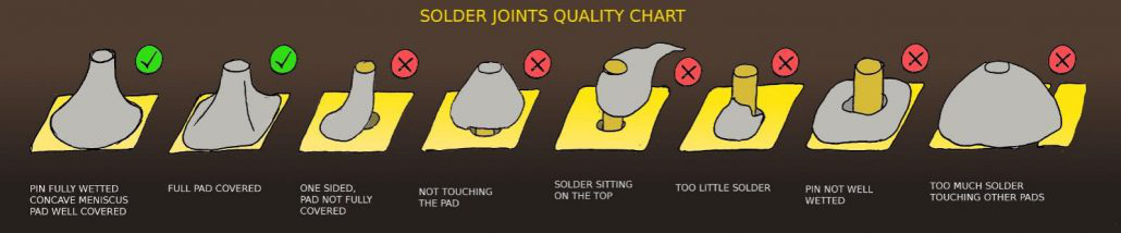
Ideal Welding Joint
In detecting welding defects, it is extremely beneficial to have an ideal welding joint image as a reference. The ideal through-hole welding joint is like a work of art.
Ideal Through-Hole Welding Joint
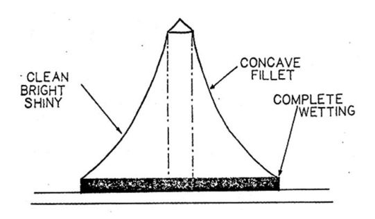
Ideally, the welding joint of a through-hole component should present a “recessed corner” shape, which forms an angle of 40 to 70 degrees with the horizontal plane and has a smooth and shiny concave surface, similar to the shape of the chocolate brand “Hershey” logo. This ideal welding joint shape can be achieved when the welding iron temperature is appropriate and the oxide layer on the PCB contact is effectively removed.
Ideal Surface Mount Welding Joint
Similarly, high-quality SMD welding joints also show smooth recessed corner characteristics.
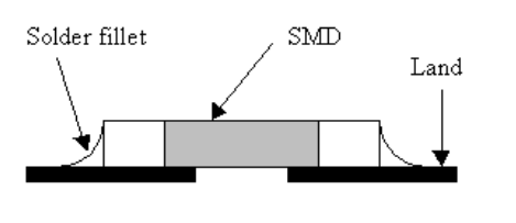
Ideal SMD welding joints
Therefore, high-quality welding joints usually have the following characteristics:
Good wettability
Concave rounded corners
Glossy and clean surface
Bad Welding Joints
Unfortunately, welding joints have many possible causes of failure, as welding tends to flow to the wrong place.
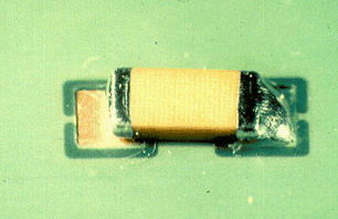
Welding joint quality of through-hole components
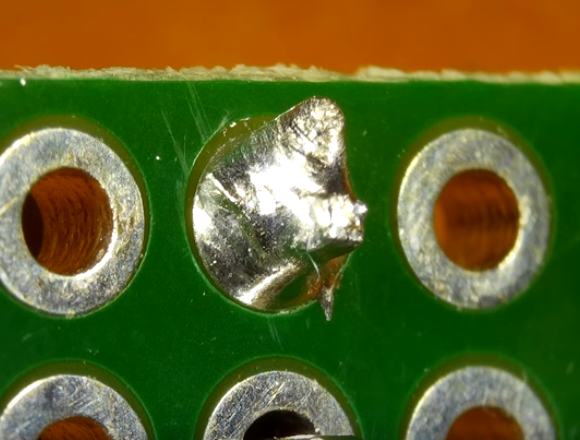
1. Welding Bridging

Welding bridges – Through-Hole and Surface Mount
Among the many problems caused by increasingly miniaturized electronic components, welding bridging is particularly prominent. When two or more welding joints are connected unexpectedly, too much welding was used during the welding, or an oversized or wide welding tip was used, resulting in an unexpected connection between the welding joints. Because the size of the welding bridge can be especially tiny, it may be difficult to identify the welding bridge. If the welding bridge is not found in time, it may cause a short circuit in the circuit, which may cause the component to burn.
For the welding bridging problem, the following repair measures can be taken: Use a welding iron to heat the center of the welding bridge to melt the welding, then carefully withdraw the welding iron to break the welding bridge structure. If the welding bridge is large, you can use a welding sucker to remove the excess welding.
2. Too Much Welding
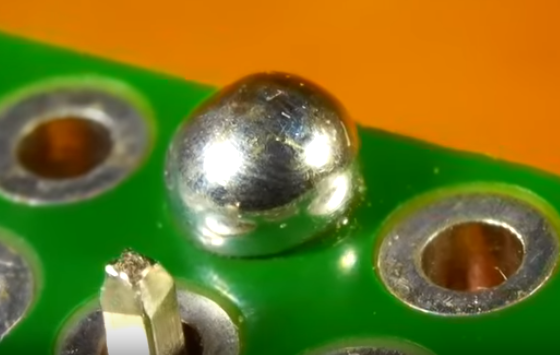
During the welding process, excess welding tends to form a buildup, which has a characteristic rounded appearance. Beginners often mistakenly believe that more welding is better, however, while increasing the amount of welding does increase the material that forms the joint, too much welding makes it difficult to identify the actual situation under the welding area. This may result in the pin or pad not being properly wetted while increasing the risk of welding bridges. Therefore, the principle of safety should be followed. Generally, the right amount of welding is enough to ensure that the pin and pad are fully wetted, and the concave surface can be kept in optimal condition, which helps achieve better joint wetting.
3. Welding Balls
Welding balls are one of the common defects in the welding process and usually occur during wave welding or reflow welding. They appear as tiny welding balls that may be attached to the laminate, resist, or conductor surface. The formation of welding balls may be caused by sundry
factors, including but not limited to improper welding paste printing technology, improper reflow temperature control, poorly printed circuit board (PCB) design, or the use of oxidized electronic components.
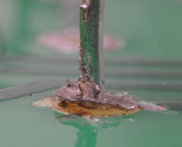
4. Cold Joints
Lumpy and Dull Cold Joints
A welding joint that appears dull and lumpy or pitted is usually caused by insufficient heat to melt the welding completely. This can be caused by a variety of factors. It may be that the welding iron or the joint is not given enough time to heat up, or the temperature setting of the welding iron is not high enough to melt the welding used (for example, lead-free welding has a higher melting point). In addition, the design of the pads and traces may also cause this problem. For instance, if the pad is directly connected to the ground plane without considering heat dissipation, the heat of the welding iron will quickly dissipate to the ground plane. If you encounter a stubborn welding joint, it indicates that the design may be defective. If appropriate measures are not taken to correct it,
5. Overheating of the Joint
Spots (more like burnt welding film)
Just as insufficient heat can cause loose joints, too much heat can cause headaches. Overheating of welding joints can be caused by setting the iron temperature too high or by the presence of an oxide layer on the pad and lead surface, which prevents the welding from flowing and heat from being effectively transferred to the welding joint. Improper heating over a long period can cause damage, which we hope is limited to flux burnout, but in more serious cases cause the pad to fall off completely, damaging the board or requiring expensive repair work. To avoid such problems, it is recommended to choose the appropriate welding iron temperature and use flux to clean joints and pads with dirty surfaces.
6. Monument
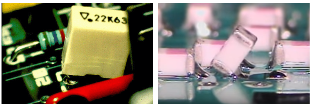
Tombstone defects typically involve surface mount components, such as resistors or capacitors, with one end lifted off the pad. Ideally, the welding should adhere evenly to both pads and begin wetting. However, if the welding wetting process on one of the pads is not worked out, one end of the component will tilt, creating a tombstone-like appearance, hence the name. Tombstone can occur during the reflow welding if the welding paste on one pad melts before the welding paste on the other pad. For example, inadequate thermal design or uneven thickness of the traces connecting the pads can cause this problem. With wave welding, larger component assemblies may be held in place in a tombstone form due to the physical push of the welding wave. Therefore, layout engineers must consider the direction of the welding wave when designing boards for wave welding.
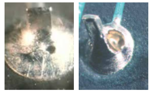
7. Inadequate Wetting (Through Holes)
Incomplete wetting of pads and pins
Incompletely wetted joints appear weak and fail to form a solid connection to the board. Ideally, the welding should completely cover the pads and pins without leaving any gaps. Inadequate wetting of pins and pads is usually caused by not applying heat to the pins and pads simultaneously, and it does not give the welding enough time to flow. Contamination of the board can also be a cause. Solutions to this problem include thoroughly cleaning the board and ensuring that the pads and pins are heated evenly.
8. Inadequate Wetting (Surface Mount)
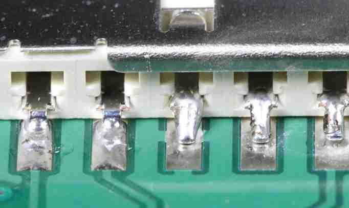
The three pins on the right are not fully wetted. Only the leads are heated, so the welding is not flowing to the pads. Similarly, surface mount devices can also face poor wetting issues. In the image shown, the three pins of a surface mount device are not wetting well on their respective pads. The weldings on the pins are not flowing to the pads because the pins are heated, not the pads. The way to fix this defect is to heat the pads with the tip of the welding iron and add more welding until the welding flows and merges with the welding already on the pins.
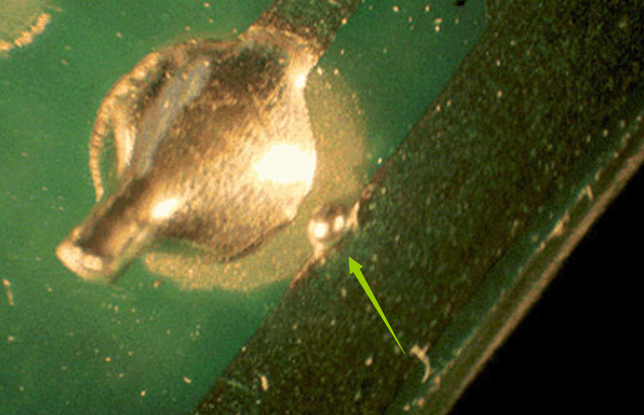
9. Welding Skip
There is a noticeable lack of welding on the left pad
A welding joint not adequately wetted by welding is often described as welding funneling. This occurs when the welding fails to cover the surface mount pad, resulting in an open circuit. The phenomenon of welding skipping can be caused by mistakes in the design or manufacturing process. This may be due to inconsistent pad sizes or the manufacturer using the wrong wave height between the board and the welding wave.
10. Pad Shedding
Lifted pads may have been separated from the PCB surface due to excessive force or heat applied to the existing welding joints. These pads are quite difficult to work with as they are extremely fragile and can easily tear away from the wire path. Every possible effort should be made to reattach the pad to the board before welding operations.
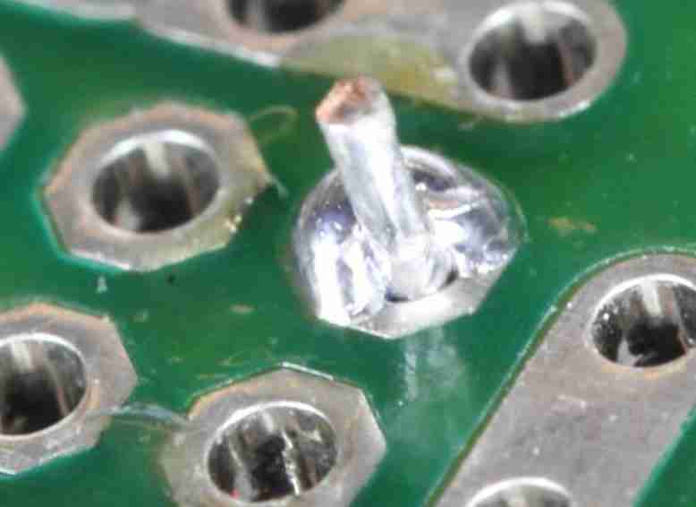
11. Welding Starvation
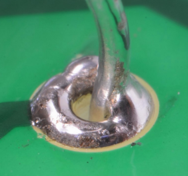
The welding does not fill the via in this image
A joint with insufficient welding will not form a solid electrical connection. In this case, the leads may not receive enough heat, resulting in a poor connection. Although the joint still has electrical contact, it may work temporarily. However, over time, cracks will gradually grow and weaken the joint, eventually causing the insufficient welding joint to fail. Fortunately, repairing an insufficiently welded joint is not difficult. Directly reheat the joint and add the appropriate amount of welding.
12. Welding Splatter/Webbing
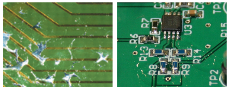
Welding splatter on traces (left) and around surface mount components (right)
Small amounts of welding splatter irregularly on the welding mask, creating a spider web-like pattern. These irregular thread-like traces are usually caused by insufficient flux or contaminants on the board surface during wave welding, which can cause short circuit problems.
13. Pin Holes and Blow Holes
Pinhole defects (left) and pore defects (right)
Pcbandassembly SMT: Pinhole and pore defects are relatively easy to identify because they appear as holes in the welding joint. The terms “pin” or “pore” provide clear information about the size of the hole, where the term “pin” specifically refers to smaller holes, and “pore” refers to larger holes. Pinholes and pores are usually not caused by wave welding, and their formation has nothing to do with the quality of manual welding techniques. Moisture on the PCB is transformed into gas by heat during the welding process. If the gas does not completely escape while the welding is still in the form of a liquid, voids may form when the welding joint solidifies. Measures that can be taken to avoid such problems include baking or preheating the circuit board to remove moisture, and ensuring that the minimum copper plating thickness in the through-hole is about 25 microns.

Get Quote Free