How to Assemble A Printed Circuit Board
Assembling a PCB involves several steps, from preparing components to soldering and testing. And it involves a systematic approach to ensure functionality and reliability.
Get Your PCB Quote!

Table of Contents
- 1. Ferramentas e materiaisPreparación
- 2. Preparación da PCB e deseño de compoñentes
- 3. Montaxe de compoñentes de orificio pasante (THT)
- 4. Montaxe de dispositivos de montaxe superficial (SMD)
- 5. Inspección e retraballo
- 6. Limpeza, probas e depuración final
- 7. Preguntas frecuentes sobre a montaxe de PCB
- 8.Summary
Electronic products are an integral part of our modern life. And PCBs (Printed Circuit Boards) are the most indispensable components of them. When you stare at these smart products, have you ever tried to make your own electronic products by hand? In fact, it is really easy to fail without a tutorial.
This article will equip you with a detailed guide to manual PCB Assembly. It covers preparation, assembling, testing, and final debugging. Furthermore, it can also applied in small-batch prototyping. Master these 6 core steps and increase the success rate by 95%!
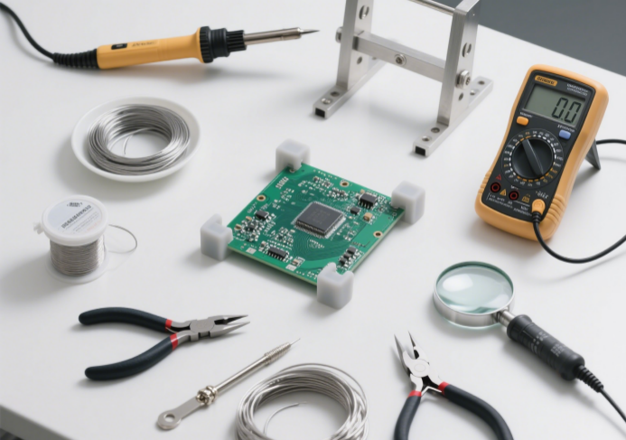
1.Tools and MaterialsPreparation
1.1 Tools Needed
(1)Essential Solder Tools:
Soldering Iron (with fine tip for SMT, thicker tip for through-hole).
Solder (rosin-core).
Flux (enhances solder flow)
(2)Auxiliary Tools:
Tweezers (for handling SMT components).
Diagonal cutters (for trimming leads).
Desoldering wick/pump (for rework).
Multimeter (for continuity and resistance testing).
PCB holder/clamp (to secure the board during assembly).
Anti-static wrist strap (to prevent ESD damage).
Magnifying Glass or Microscope (for tiny SMT components, optional).
1.2 Materials
Blank PCB (with copper traces and pre-drilled holes)
Electronic components (resistors, capacitors, ICs, connectors, etc., sorted by type and value)
Solder Paste (for SMT components, if using reflow soldering).
Isopropyl alcohol and cotton swabs (for flux residue cleaning)
2.PCB Preparation and Component Layout
2.1 PCB Preparation
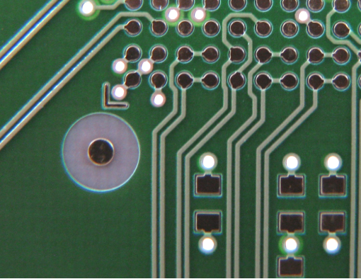
(1)Inspect the PCB: Check for manufacturing defects (missing pads, shorted traces, misprinted silkscreen, etc.).
(2)Electrical Continuity Test: Check the continuity with the multimeter.
(3)Insulation Test: Measure resistance between adjacent signal traces.
2.2 PCB Cleaning
(1)Contamination Removal: Use IPA to clean oil/fingerprints. Ultrasonic clean old flux residue with a neutral detergent.
(2)Pad Pre-Treatment: Remove oxidation and protect the solder mask.
2.3 Aid for Positioning and Marking
(1)Fiducial Marking
Optical Fiducials (for SMT): Add three copper marks at PCB edges for pick-and-place machine alignment.
Manual Alignment: Draw crosshairs at PCB corners with a marker. And align it with grid paper on the workbench for uniform component orientation.
(2)Special Area Preparation
BGA Pads: Inspect for pad flatness under magnification; reject boards with too large a depression to avoid solder bridging.
For THT:
Oxidized pads: Sand and activate with flux via soldering iron.
Damaged pads (copper loss <30%): Bridge to adjacent vias with jumper wires for electrical continuity.
Through-Holes: Deburr clogged vias with a reamer to ensure smooth lead insertion.
Hole Diameter Matching: Maintain a 0.2–0.4mm difference between lead diameter and via diameter (too small causes insertion force issues, too large causes wobbling).
For SMT:
Remove fingerprints and oil stains: For electroless nickel immersion gold (ENIG) pads, clean them with a cotton swab dipped in isopropyl alcohol (IPA).
Activate with flux: For hot air solder leveling (HASL) pads, if the pads appear gray (to improve solder wettability).
2.4 Component Layout
(1)Schema and Layout Review:
Cross-Verify Schematic and PCB Silkscreen: Confirm component designators match their footprints. Verify no missing test points or redundant footprints. Confirm component placements, polarities (diodes, capacitors, ICs), and orientations.
(2)Component Preprocessing:
THT Components:
Clean lead oxidation with sandpaper or a wire brush;
bend leads to align with PCB holes (adjust spacing with pliers if needed).
SMT Components:
Use a magnifying glass to check the terminals of components (if oxidized, clean silver terminals with absolute ethanol);
handle with tweezers to avoid touching pads;
ground yourself with an anti-static strap when handling sensitive components (ICs) to prevent ESD damage;
for QFP/SOP-packaged ICs, confirm the coplanarity of the leads (correct it with a leveling tool to avoid cold joints, if needed).
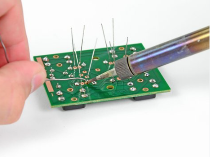
3.Through-Hole Components (THT) Assembly
3.1 Components Inserting
(1)Start with Short/Low Components: Install shorter components first (resistors, small capacitors) to avoid blocking access to adjacent pads.
(2)Align Pins with Pads: Push component leads through the PCB holes from the top (component side), ensuring they protrude slightly on the solder side.
(3)Secure Components: For tall components (connectors, transformers), use a clamp or hold them in place temporarily.
(4)Orientation Alignment: Ensure components are inserted in the correct direction (reverse installation may burn components).
3.2 Soldering
Preheat pad: Contact pad and lead simultaneously with the iron tip (45° angle) until the pad edge slightly darkens.
Apply Solder: Feed the solder to the joint (not the iron) until a small, shiny fillet forms.
Avoid over-soldering (excess solder can cause bridges).
Remove Iron: Wait ~1 second for the solder to solidify before moving the board.
3.3 Leads Trimming
Use flush-cutting pliers to trim excess leads close to the solder joint (leave ~1mm to prevent pad lifting).
ESD Control: Clean trimmings immediately with a sticky mat or compressed air to prevent metallic debris shorting.
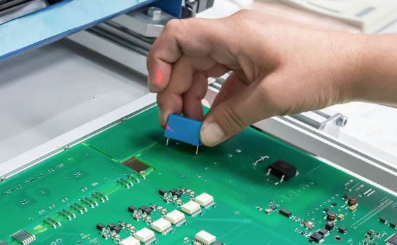
4.Surface-Mount Device (SMD) Assembly
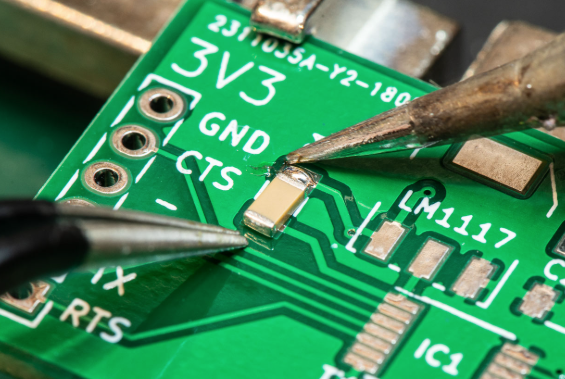
4.1 Hand Soldering (for small quantities)
(1)Apply Flux: Dab a small amount of flux on the PCB pads (optional if using flux-core solder, but helps with wetting).
(2)Place Components: Use tweezers to position SMT components (0402 and larger) on their pads, aligning pins with the pad (check polarity for diodes, capacitors, and ICs).
(3)Tack Solder One Pin: Secure the component by soldering one corner pin first, then recheck alignment and adjust if needed.
(4)Solder Remaining Pins: For QFP/SOIC ICs, gently drag the iron tip along the pins, feeding the solder as needed. For 0603/0805 components, solder one pad, place the component, and then solder the other pad.
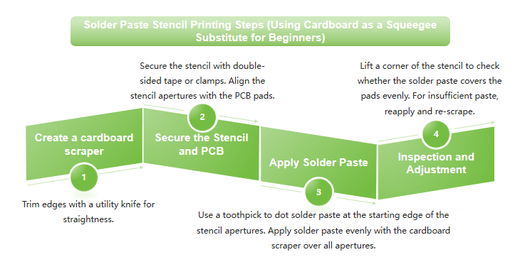
4.2 Solder Paste + Reflow (for larger batches)
(1)Apply Solder Paste: Use a stencil and squeegee to deposit paste on SMT pads.
Place Components: Use a pick-and-place tool or tweezers to position components on the paste.
(2)Reflow: Heat the board in a reflow oven or with a hot air station to melt the paste, following the temperature profile for the paste used.
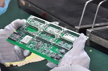
5.Inspection and Rework
5.1 Inspection
(1)Visual Inspection
| Inspection Item | Acceptance Criteria | Common Defects and Identification |
| Solder Joint | Shiny, concave half-moon shape; no burrs or bridging | Cold joints (dull, granular surface), solder bridging (adjacent pads connected), insufficient solder (pad edge exposed) |
| Component | Correct polarity; no displacement |
Tilted components, reversed polarity (IC misaligned), missing parts (BOM list mismatch) |
| Pads and Traces | No pad delamination; no trace shorts/opens | Damaged pads (copper loss >30%), trace spacing <0.1mm (short risk) |
| Flux Residue | No obvious white/yellow residue around joints | Excessive sticky residue (potential conductive corrosion) |
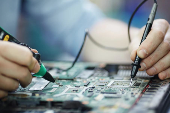
(2)Continuity Test: Use a multimeter to verify connections between pads and component leads (ensure no opens or shorts).
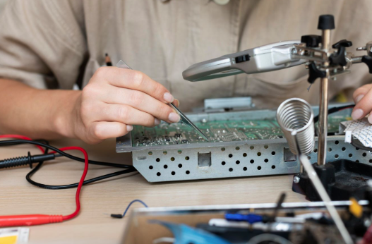
5.2 Rework
(1)Component Replacement:
Through-Hole Components: Use a desoldering pump or solder wick to remove old solder. Gently pull out the component while heating the joints.
SMD Components: Apply hot air to the component using a rework station. Lift the component with tweezers once the solder liquefies. Clean the pads, apply the new paste, and solder the replacement part.
(2)Pad Delamination/Damage:
Mild Damage (Copper Loss <50%): Clean the area, apply thin flux, and bridge to an adjacent pad/net with an enameled wire (secure with high-temperature tape to prevent stress fracture).
Complete Pad Loss: Identify the pad’s inner-layer trace or via, soldering the lead directly to exposed copper (reinforce with silicone adhesive for mechanical strength).
(3)THT Cold Joints/Bridging:
Solder Bridging (Short Circuits): Apply flux to the bridged area.
Place the solder wick over the bridge and heat with the iron until excess solder is absorbed.
Cold Solder Joints: Add flux to the joint. Reflow with the soldering iron until the solder flows smoothly.
(4)SMT Misalignment/Bridging:
Component Misalignment (Terminals Not Fully on Pads): Heat the component with a hot air station until the solder melts, realign with tweezers.
QFP Fine-Pitch Bridging: Use an ultra-fine iron tip with minimal solder, swiping along lead gaps to separate joints via surface tension. For extensive bridging, first, remove excess solder with a wick, then re-solder each lead.
5.3 Post-Rework Processing
(1)Residue Cleaning: Wipe reworked areas with isopropyl alcohol to remove flux and metallic debris (prevent long-term corrosion).
(2)Secondary Inspection: Recheck repaired joints visually and for continuity; retest complex IC functionality.
6.Cleaning, Testing, and Final Debugging
6.1 Cleaning
(1)Purpose of Cleaning:
Remove flux residues, solder splatter, and contaminants to prevent:
Corrosion or dendritic growth;
signal interference;
poor adhesion of conformal coatings.
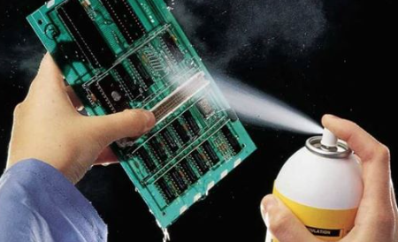
(2) Steps for Manual Cleaning:
Apply IPA to contaminated areas.
Gently scrub with a brush or swab.
Dry with compressed air or a lint-free cloth.
Inspect under UV light (optional) to detect residual flux.
Caution:
Avoid acetone on plastics or silkscreen labels.
Use ESD-safe brushes for sensitive components.
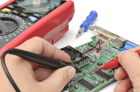
6.2 Testing
(1)Critical Pre-Power Safety Check
Power-Ground Short Detection: Use a multimeter measure between VCC and GND. If the resistance is too small, immediately power off and check: Reverse-installed electrolytic capacitors; bridged IC power pins; and exposed traces from pad delamination (inspect dense pad areas with a magnifier).
Continuity Verification: Randomly test 10% of components for solder joint-lead connectivity (buzzer in continuity mode indicates good contact), prioritizing easily missed SMT parts.
(2)Automated Optical Inspection (AOI):
Industrial Use: High-resolution cameras scan boards against CAD data to detect missing/misaligned components.
DIY Alternative: Use open-source software with a USB microscope for basic pattern recognition.
(3)X-Ray Inspection: Detect hidden defects in BGA, QFN, or via-in-pad structures. Identify voids in solder balls or insufficient underfill.
(4)In-Circuit Test (ICT): Validate component values (resistance, capacitance) and signal paths.
(5)Functional Test: Power up the board and verify operational performance.
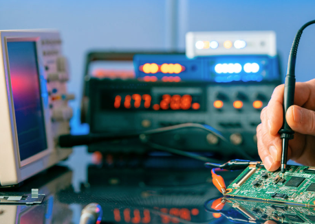
6.3 Debugging
(1)Common Failure Modes:
Power Issues:
Symptoms: No power, voltage drops.
Debugging: Check regulator outputs, diode orientations, and fuse continuity.
Signal Integrity Problems:
Symptoms: Glitches, EMI.
Debugging: Add decoupling capacitors, and reroute noisy traces.
Firmware/Software Bugs:
Symptoms: MCU freezes, communication errors.
Debugging: Use JTAG debuggers, and review code/logs.
(2)Step-by-Step Debugging Process:
Isolate the Issue:
Divide the PCB into functional blocks (power, analog, digital).
Test each block individually.
Signal Tracing:
Use an oscilloscope to follow signals from input to output.
Component-Level Checks:
Replace suspected faulty components (e.g., swapped ICs).
Environmental Testing:
Test under extreme conditions (temperature, vibration) if applicable.
7.PCB Assembly FAQs
The increase in the number of soldering will greatly reduce the corresponding material strength and material properties. It will also cause pad delamination. This will eventually affect the failure of the solder joint.
Buzzer indicates continuity (<1Ω); silence signals cold joints or opens (requiring reflow).
Because grease can cause solder paste to fall off.
Shorter/smaller components first, taller/larger components last.
No. They will corrode PCBs.
By balancing design complexity, component selection, and assembly volume, you can optimize costs while meeting project requirements.
Check for thermal expansion mismatches or marginal solder joints.
Reflow the joint with fresh solder and flux.
The time required to assemble a printed circuit board (PCB) depends on design complexity, component availability, assembly type, and order volume.
The root cause of resistance deviation from misoriented color bands is the inversion of significant digits and multipliers, leading to erroneous mathematical combinations.
8.Summary
The PCB assembly is a fascinating but complex journey. It transforms a simple electronic circuit design into an actual working component. Each step of the PCB assembly process is crucial to creating high-quality boards. This includes the initial design check, assembly, final quality checks, and final verification. In today’s technologically-driven world, PCB assembly skills are essential for anyone working on a high-volume electronic prototype.

Get Quote Free