PCB Panelization Standard in PCB Manufacturing
Get Your PCB Quote!

Table of Contents
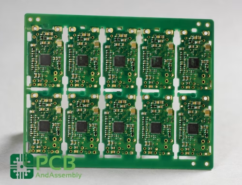
There is no doubt that PCB assembly is an extremely complex task that requires the highest levels of skill and efficiency. One thing that goes a long way in aiding the process is panelization. In simple terms, panelization means grouping boards together, which increases the speed of processing. Panelization is especially common in high-volume transactions and when orders are being processed quickly, and optimization is important. Smaller boards are joined together, making it much easier to get them across the assembly line. These boards can then be easily removed later.

The Process of Panelization Usually Proceeds as Follows
The first step involves the manufacturer making blank boards.
Next, the designer arranges these boards onto a larger board. Depending on the complexity of the circuit, the number of layers may exceed 42. This is easier if the boards have a regular shape, as odd shapes can make the layering process difficult.
And then processed as one consolidated panel. This means that the machine can easily fix the components to the board.
However, It Is Important to Consider the Following Points
1. Array strength – Generally, increasing the number of boards in each array increases the overall strength.
2. Layout – It is important to consider the location of sensitive components towards the edges.
3. Shape – This is a good choice when you process rectangular shapes.
4. Tool holes – The array can often provide space for tool holes for automated testing.
Advantages of PCB Panelization
With PCB panelization, production efficiency is greatly increased. Some of the advantages of panelization include:
1. Batch production – This is particularly useful for optimizing batch production while meeting time and saving money
2. Safety – Assembly often involves a lot of vibration. This is why panelization protects PCBs from corrosion
3. Speed – When processing multiple boards at a time, speed is a given. Both welding and testing processes become faster
However, some limitations to panelization include the fact that it is not too useful for low-volume PCB manufacturing. In addition, panelization is also limited by the following factors:
1. Board thickness
2. Component weight
3. Space between boards
To ensure panelization efficiency:
1. The dimensions of the boards should be similar
2. Overall, the parameters of the board must be similar
3. There should be a similar copper distribution
There Are Several Different Ways to Accomplish Panelization:
1. V-groove panelization: This involves making V-shaped lines between boards and is useful when there are no overhanging parts
2. Breakaway tabs: This is a method of punching holes between individual boards.
Whether V-score or tab routing methods should be used depends largely on the design.
3. Shape: Generally, V-score is suitable for regular shapes, while tab routing is suitable for unusual shapes.
4. Edge components: Tab routing may be better than v-score for components close to the edge.
5. Edge Quality: Tab routing is preferable in terms of edge quality
6. Time V scoring works better from the perspective of time required.
7. Waste: V scoring is preferable in terms of material waste as it reduces wasted material, thus reducing the overall cost per board.
Here Are Some Fey Guidelines to Follow for Panelization
1. For routing rectangular panelization with sides greater than 1.00 inches, you must add 100 mils between PCBs and a 400 mil border on the outside. However, if the length is shorter, you need to add 300 mils between PCBs
2. For non-rectangular PCBs, you need to add 300 miles of space.
3. In the case of V scoring, you need to maintain 20 mils of space between the edge of the PCB board and the trace, and 300 mils on opposite sides.
However, there are some exceptions to the above rule of thumb:
4. To ensure that depanelization does not result in component damage, the border between PCBs demands to include the stick-out distance.
5. To increase the mechanical strength of the panel in case the components are heavy, additional material demands to be added between the panels.
Another rule of thumb to follow is that when routing is done, the clearance between the metal and the PCB board needs to be 5 mils. However, in the case of V-rating, it needs to be as much as 20 mil.
Also in the case of using paging tabs, what needs to determine how many paging tabs should be used is the size and shape of the board.
Depaneling
After SMT processing and testing are completed, the next step is depaneling. Depending on the panelization method chosen, depaneling or dividing into different parts can be done in sundry ways. Some of them include:
1. Breaking by hand
2. Cutting along the V-groove
3. Saw marks
4. Laser cutting
5. Punching out the board, etc.
Shenzhen Pcbandassembly SMT Processing: In summary, panelization must be considered when designing. This will ensure have to deal with the least delays and avoid too many redesigns.

Get Quote Free