How to Repair a Broken PCB Trace Using a Jumper Wire
A cracked PCB trace doesn't have to mean a scrapped board. Follow this step-by-step jumper wire repair guide — with critical precautions and verification checks at every stage.
Get Your PCB Quote!
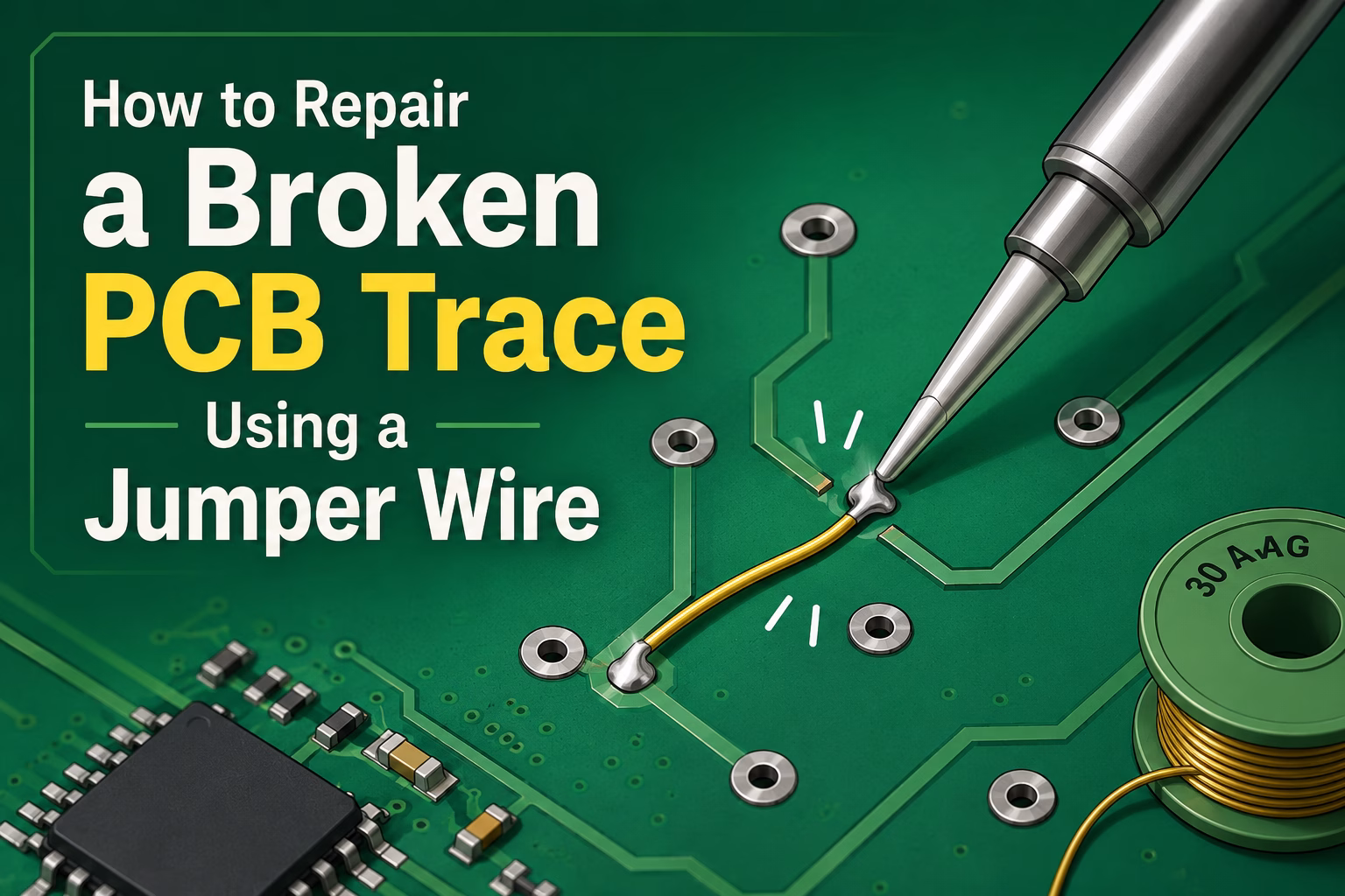
Table of Contents
- 1. Die technische Logik der Leiterbahnreparatur
- 2. Werkzeuge des Handwerks: Mehr als die Grundlagen
- 3. Drahtauswahl: Anpassung von Stromstärke und Impedanz
- 4. Schritt für Schritt: Das Standardverfahren IPC-7721
- 5. Die Physik des Scheiterns: Warum Verankerung unverzichtbar ist
- 6. Hochfrequenz- und Hochstrombetrachtungen
- 7. Häufige Reparaturfallen
- 8. Zusammenfassung
A few months ago, a client sent us a high-value industrial control board that had been “repaired” in the field. To the naked eye, the fix looked reasonable: a thin strand of copper wire bridging a 5mm gap in a power rail. However, the board failed again after just 48 hours of operation. When we put it under the microscope, the failure was classic: the solder joint hadn’t actually broken, but the trace itself had delaminated further back from the repair site. The technician had made a fundamental mistake—they hadn’t accounted for the Coefficient of Thermal Expansion (CTE) mismatch between the FR-4 substrate and the jumper wire.
In the PCB industry, we often see trace repairs treated as a simple soldering task. In reality, it is a mechanical engineering challenge. When a board heats up from 25°C to an operating temperature of 70°C, the copper and the epoxy glass expand at different rates. Without a specific strain-relief “U-loop” and proper anchoring, a jumper wire acts like a lever, slowly prying the remaining copper trace off the board with every thermal cycle. At PCBAndAssembly, we treat every trace repair as a restoration of structural integrity, not just electrical continuity.
1. The Engineering Logic of Trace Repair
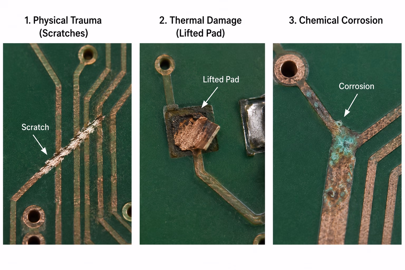
When we talk about repairing a broken trace, we are usually dealing with one of three scenarios: physical trauma (scratches), thermal damage (lifted pads from overheating), or chemical corrosion. Each requires a different mindset . A scratch on a 0.5mm signal trace is an easy fix; a vaporized 2oz copper power plane is a reconstruction project.
The primary goal is to restore the original electrical characteristics— specifically resistance and, in high-speed designs, impedance—without introducing new failure modes. We have found that the most common cause of ” re-repair” is the “glob” method: applying a massive amount of solder over a break. Solder is a brittle interconnect, not a structural material. Over time, vibration and thermal expansion will cause micro-cracks in a solder- only bridge. This is why the industry relies on jumper wires for anything beyond a hairline fracture.
When to Repair vs. When to Scrap
Professional judgment is required before starting. If a board has suffered a ” charring” event where the FR-4 substrate is blackened, the carbonized material is now conductive. Simply bridging the trace won’t work because the board itself will now leak current between layers. In our experience, if the carbonization extends deeper than 0 .2mm into the substrate, the board should be scrapped or the affected area must be completely milled out and replaced with an epoxy plug —a process that is rarely cost-effective for standard commercial boards.
2. Tools of the Trade : Beyond the Basics
You cannot perform a reliable trace repair with a 100-watt plumbing iron and a pair of kitchen scissors. Precision is mandatory. We’ve seen drill-wander and trace damage increase by 40% when technicians use dull steel scalpels instead of carbide-tipped scribes for removing solder mask. Carbide maintains a sharp edge longer , allowing for a clean, perpendicular cut into the mask without “smearing” the epoxy glass underneath.
The following table outlines the minimum viable toolset for a repair that meets IPC-A-610 Class 3 standards (High Performance/Harsh Environment Electronics).
| Tool/Material | Specification | Purpose |
| Soldering Station | Digital Temperature Controlled (±5°C) | Prevents overheating and pad lifting during the repair. |
| Solder Alloy | SAC305 (Sn96.5/Ag3.0/Cu0.5) | Standard lead-free alloy; prevents intermetallic brittleness on modern boards. |
| Flux | No-Clean or Rosin-Activated (Type ROL0) | Essential for breaking surface oxides on aged copper. |
| Abrasive Tool | Carb ide Scribe or Fiberglass Pen | Safely removes solder mask without thinning the copper trace. |
| Cleaning Agent | 99.9% Isopropyl Alcohol (IPA) | Rem oves skin oils and flux residues which cause long-term corrosion. |
| Encapsulant | UV-Curable Epoxy or Polyimide Tape | Mechanical anchoring of the wire to the substrate . |
Table 1: Professional Trace Repair Tooling & Materials
3. Wire Selection: Matching Current and Impedance
A frequent mistake is choosing a wire based solely on what is available on the bench. If you use a 34 AWG wire to repair a trace that carries 5 Amps, that wire will act as a fuse. Conversely, using a heavy 22 AWG wire on a fine 0.1mm signal trace creates a massive “heat sink” effect, making it nearly impossible to get a good solder joint without damaging the surrounding board area.
We use the following cross-reference at PCBAndAssembly to ensure that our jumper wires match the current-carrying capacity of the original copper traces. Note that these are based on 1oz (35µm) copper thickness, which is the industry standard for most internal and external layers.
| Trace Width (Inches) | Trace Width (mm) | Equivalent Wire Gauge (AWG) | Max Current (A ) – 10°C Rise |
| 0.01 0″ | 0.25 mm | 34 AWG | 0.5 A |
| 0.020″ | 0.5 0 mm | 30 AWG | 1.2 A |
| 0.050″ | 1.27 mm | 26 AWG | 2.5 A |
| 0.100″ | 2.54 mm | 22 AWG | 5.0 A |
Table 2: Trace Width to Solid Wire Gauge (AWG) Equivalents
For high-frequency signals (above 100 MHz), the geometry of the jumper wire matters significantly. A round wire has different inductance than a flat trace. In these cases, we recommend keeping the jumper as short as possible—ideally less than 1/10th of the signal’s wavelength—to avoid creating a “stub” that causes signal reflections.
Need PCB Manufacturing or Assembly?
Get a free quote within 24 hours. We specialize in prototype-to-production PCB/PCBA for hardware teams worldwide.
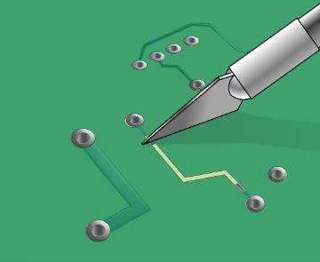
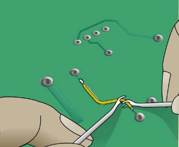
4. Step-by-Step: The IPC-7721 Standard Procedure
Following the IPC-7721 standard isn’t just about following rules; it’s about following a sequence that has been proven across millions of flight-critical and industrial boards. Each step below includes a Critical Precaution—the specific thing most likely to go wrong—and a Verification check so you know you’re ready to move on before you do.
Step 1: Preparation and Inspection
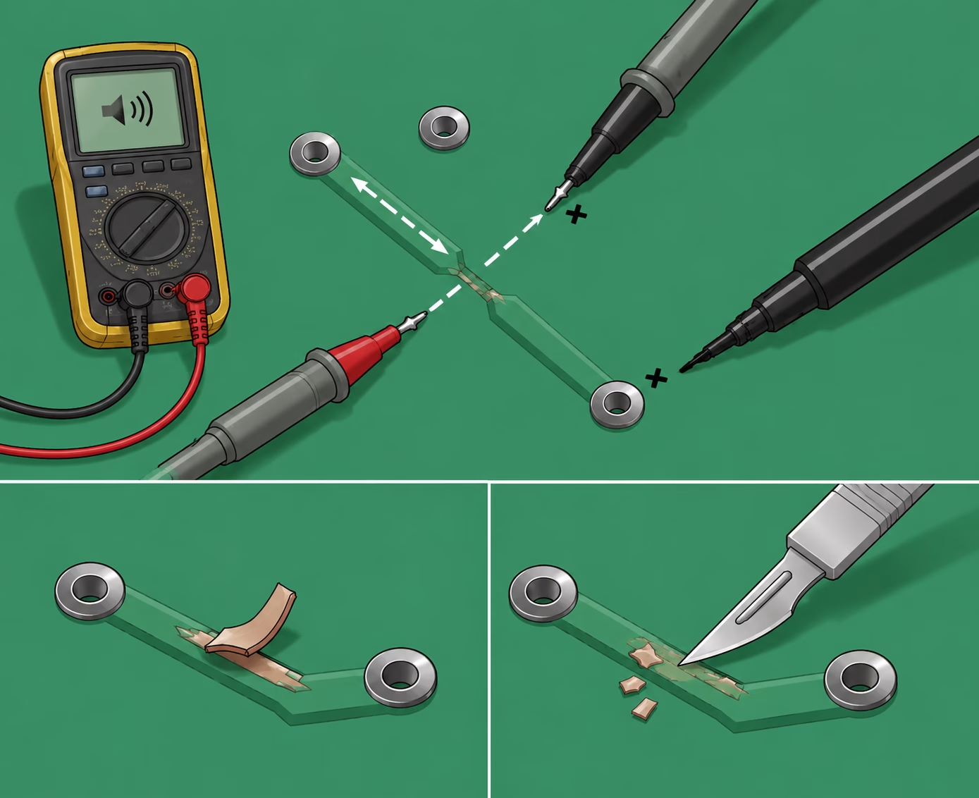
Set your multimeter to continuity mode and probe outward from the visible damage in both directions until you locate the last two points that should be connected but are not. Mark them with a fine-tip marker. If any copper is visibly delaminated—lifting away from the substrate—use a sharp blade to trim it flush. A loose copper flap is not a repair candidate; under vibration it can migrate, bridge an adjacent net, and create a short that is far harder to diagnose than the original break.
Critical Precaution: Confirm that only the target trace is open. Probe all immediately adjacent traces to verify they remain continuous and isolated from the broken net. A secondary break or a pre-existing short that you have not identified will make the repair appear to fail even when executed perfectly.
Verification: Multimeter confirms open circuit across the break and continuity on all adjacent nets. Only then proceed.
Step 2: Exposing the Copper
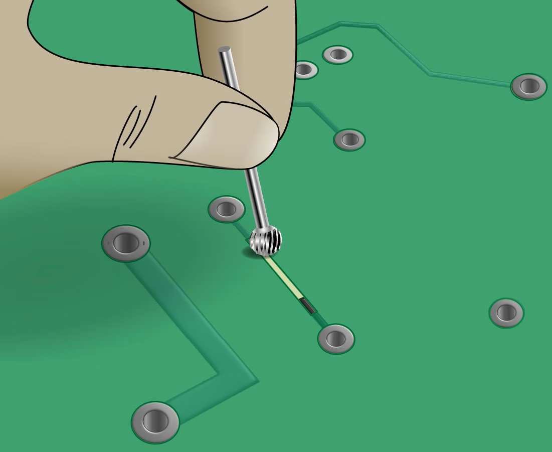
Using a carbide-tipped scribe—not a steel scalpel, which dulls rapidly and smears the epoxy glass—scrape away the solder mask to expose at least 1.5 mm × 1.5 mm of bare copper on each side of the break. Work at a shallow angle of approximately 15° to the board surface. This keeps the blade cutting the mask rather than gouging into the copper foil beneath it.
Critical Precaution: Do not scrape perpendicular to the board or apply downward pressure. Undercutting the copper foil—thinning it from below—creates a stress point that will crack under thermal cycling even if the jumper itself is perfect. IPC-6012E sets the maximum allowable undercut at 0.05 mm.
Verification: Inspect under 10x magnification. The exposed copper should be bright and uniform with no gouges, scratches running across the grain, or areas where the foil looks thinner than the surrounding copper.
Step 3: Cleaning and Fluxing
Wipe both exposed pads thoroughly with >90% isopropyl alcohol (IPA) on a lint-free wipe such as a Kimwipe. Allow to dry completely—typically 20 to 30 seconds—before proceeding. Then apply a small amount of no-clean, rosin-activated flux (such as Kester 951 or MG Chemicals 8341) to each pad. Tacky flux is preferred over liquid flux here because it holds the wire in position during the initial tack solder, giving you a free hand.
Critical Precaution: Do not touch the cleaned pads with bare fingers. Skin oils contain chloride salts that, when heated during soldering, react with the flux to form a conductive residue. That residue can cause leakage current between adjacent nets and, over time, dendritic growth that leads to intermittent shorts. We have measured a 15% increase in joint resistance over the first year of service on repairs where this step was skipped.
Verification: The exposed copper should appear bright with a slight sheen from the flux. If the surface still looks dull or has a dark tint, repeat the IPA wipe; residual oxidation will prevent proper solder wetting in the next step.
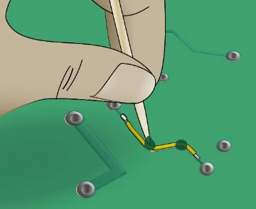
Step 4: Selecting and Preparing the Wire Jumper
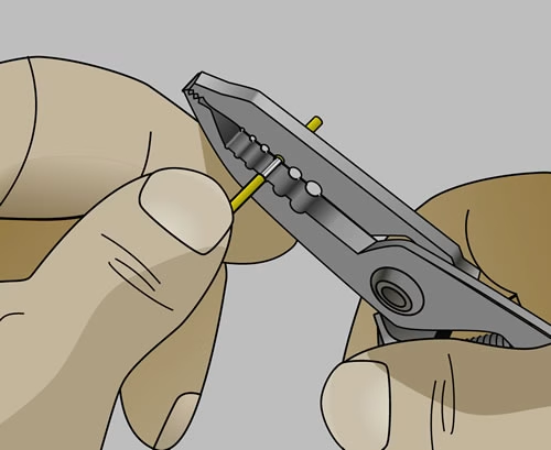
Select a solid-core, tinned copper wire matched to the current capacity of the original trace—refer to the wire gauge table in Section 3. Never use stranded wire; individual strands work-harden independently under vibration and the wire will fail at the bundle long before a solid conductor would. Using a precision wire stripper (such as the Ideal 45-121), strip exactly 2.0 mm of insulation from each end without nicking the copper. Then tin 1.0 mm of each stripped end with SAC305 solder. Hold the wire with a third-hand tool or vacuum pickup during this step; skin oils on the wire ends will degrade solderability at the joint.
Critical Precaution: Set the iron to 320–340°C for SAC305 alloy (per IPC-J-STD-001G, Section 5.3). Do not use a higher temperature to speed up tinning—excess heat will burn the flux before it can do its job, leaving a dull, grainy tin coat that will form a weak bond at the pad.
Verification: Each tinned end should be smooth and bright, not lumpy or grey. Measure resistance end-to-end on the wire with a multimeter—it should read well under 1 Ω for any gauge listed in the selection table. A high reading at this stage means a poor tin coat or a nicked conductor; replace the wire rather than proceed.
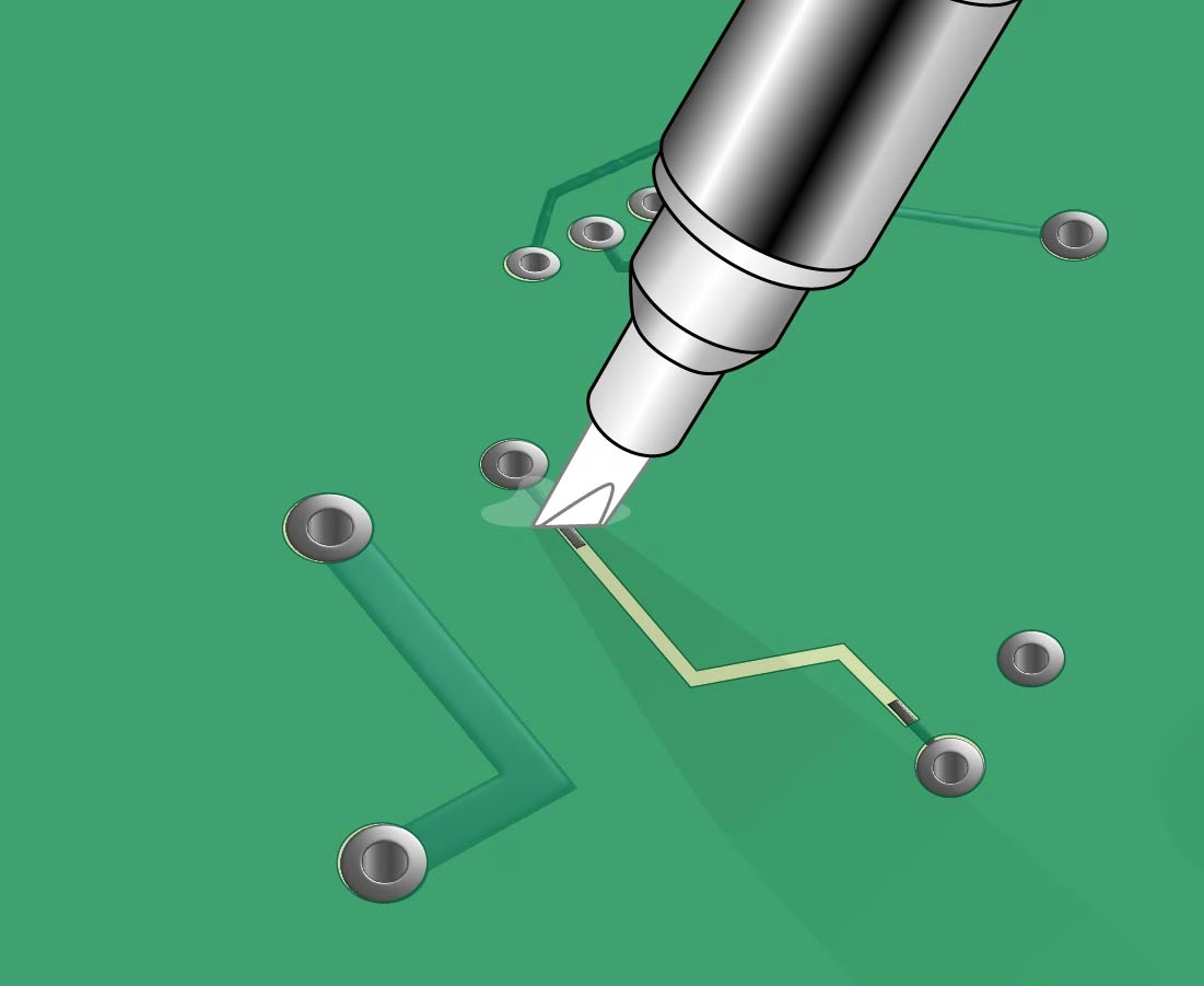
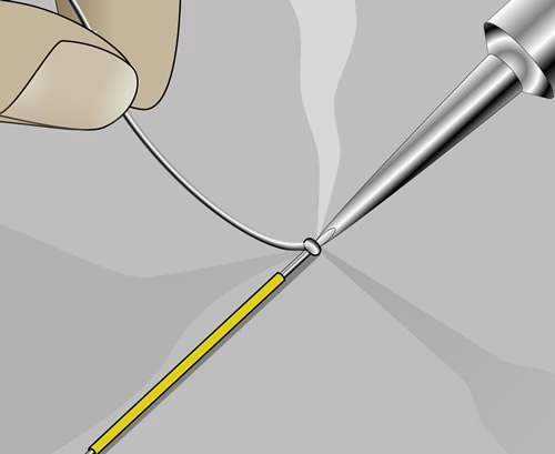
Step 5: Soldering the First End
Anchor the wire to the more structurally stable of the two pads first—avoid pad locations near connector flex points or board edges, which experience the highest mechanical stress in service. Using the drag soldering method, touch the iron tip to the fluxed pad and allow it to reach temperature for approximately one second, then gently feed the pre-tinned wire end into the molten pool. Remove the iron smoothly without dragging the wire. Hold the wire absolutely still for at least three seconds while the joint solidifies; any movement during cooldown will produce a cold joint.
Critical Precaution: Keep total iron dwell time on the pad under 2 seconds. The epoxy-glass bond between the copper foil and the FR-4 substrate begins to degrade above 130°C. Prolonged heat—even at a correct tip temperature—will transfer enough energy into the board to weaken that bond, causing the pad to lift either immediately or during the first thermal cycle in service.
Verification: Under 10x magnification, the fillet must cover at least 75% of the wire circumference and show a smooth, concave wetting profile with a 30°–45° contact angle (per IPC-A-610H, Section 8.2.1). No voids, solder balls, or mask discolouration around the joint perimeter. If any are present, reflow with fresh flux rather than adding more solder.
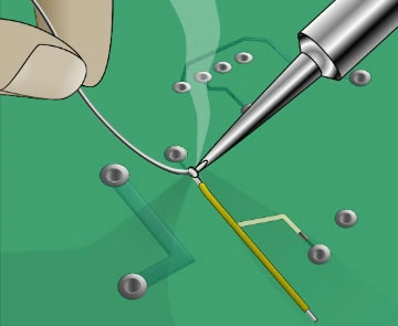
Step 6: Forming the Wire and Securing It to the Board
Route the free end of the wire along the original trace path—never perpendicular to it, which creates a stress riser at the joint. Give the wire a gentle upward bend at the midpoint to form a shallow “U” or hump. This loop is not cosmetic: FR-4 substrate expands at roughly 14 ppm/°C while copper expands at 17 ppm/°C. Over hundreds of thermal cycles that mismatch accumulates. The U-loop absorbs it as elastic flex rather than transferring the load to the solder joints. Maintain a minimum clearance of 0.5 mm from all adjacent traces and components along the entire wire length.
Once the routing is correct, apply two small dots of UV-curable epoxy (such as Loctite 3108 or Dymax 9-20502) at the one-third and two-third points along the wire. Cure under a 365 nm UV lamp for 30 seconds. Do not place epoxy over the solder joints themselves—this prevents future inspection and makes rework nearly impossible.
Critical Precaution: Do not substitute hot glue or RTV silicone for UV-curable epoxy. Silicone-based materials absorb up to 2% moisture by weight (per JEDEC JEP182), which promotes galvanic corrosion at the copper surface in any environment with humidity above 60% RH—a common condition in industrial and outdoor enclosures.
Verification: The epoxy dots should be fully cured—firm and non-tacky to a toothpick. The wire should not shift when gently pressed sideways. Confirm the U-loop shape is intact and that the wire clears all adjacent components by at least 0.5 mm.
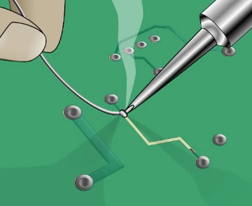
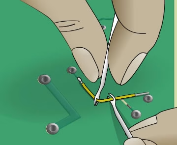
Step 7: Soldering the Second End
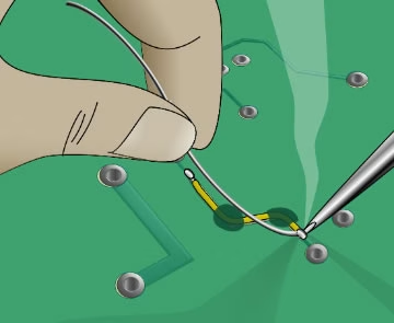
With the wire body anchored, solder the second end using the same drag technique as Step 5. Re-apply flux to the pad if the earlier application has dried. Touch the iron to the pad, allow one second to reach temperature, then draw the pre-tinned wire end into the joint. Because the wire is now fixed and both surfaces are pre-tinned, the bond forms quickly—dwell time should not exceed 1.5 to 2 seconds.
Critical Precaution: The anchored wire means there is no give if you apply lateral pressure with the iron tip. Keep the iron moving only vertically—straight down to the pad and straight up to withdraw. Dragging the tip sideways at this stage can lever the wire against the cured epoxy dot and crack it, destroying the strain relief you just built.
Verification: Apply the same visual standard as Step 5—smooth concave fillet, 75% wire circumference coverage, no voids or mask burns. Then gently tug the wire lengthwise with a toothpick. Neither joint should show any movement. If the second joint lifts at all, it has insufficient solder or a cold bond; reflow immediately before the epoxy is stressed further.
Step 8: Final Electrical and Visual Sign-Off
A repair is not complete until it is verified against objective, measurable criteria—not just a visual impression. Perform all four checks below before returning the board to service.
- Electrical continuity:Resistance across the repair must be below 0.05 Ω. For power traces, use a four-wire Kelvin measurement to exclude probe contact resistance from the reading. A result above 0.1 Ω indicates residual oxidation at one of the joints; reflow with fresh flux.
- Isolation resistance:Apply 50V DC between the repaired net and each adjacent net using an insulation tester. Isolation must exceed 1 MΩ. This catches hairline solder bridges that are invisible to the naked eye and would not show up on a standard continuity check.
- Mechanical integrity:Probe both solder joints and the wire body gently with a toothpick. Zero movement is the only acceptable result. Any rocking at a joint means the fillet is either cold or bonding only partially to the pad surface.
- Visual inspection:Under 10x magnification, confirm no bridging to adjacent pads, no lifted or discoloured solder mask around either joint, and no micro-cracks visible in the fillet surface. Photograph the finished repair and record the wire gauge, solder alloy, epoxy product, and test results. If this board returns for service, that documentation is the first thing the next technician will need.

About PCBAndAssembly
Time is money in your projects – and PCBAndAssembly gets it. PCBAndAssembly is a PCB assembly company that delivers fast, flawless results every time. Our comprehensive PCB assembly services include expert engineering support at every step, ensuring top quality in every board. As a leading PCB assembly manufacturer, we provide a one-stop solution that streamlines your supply chain. Partner with our advanced PCB prototype factory for quick turnarounds and superior results you can trust.
5. The Physics of Failure: Why Anchoring is Non- Negotiable
A jumper wire is a high-mass object compared to a copper trace. If the board is subjected to vibration—common in automotive or industrial applications—the wire will vibrate like a guitar string. This vibration concentrates all the mechanical stress at the two solder joints. Eventually, the copper will suffer from “work hardening” and snap at the heel of the solder fillet.
To prevent this, the jumper wire must be anchored to the board. At PCBAndAssembly, we use a two-part approach for critical repairs:
- Temporary Holding:Use small strips of Kapton (polyimide) tape to hold the wire in its “U-loop” shape while soldering the second end.
- Permanent Encapsulation:Once the electrical connection is tested, apply small dots of UV-curable epoxy every 5mm to 10mm along the wire’s length. Avoid putting epoxy directly over the solder joints themselves, as this makes future inspection or rework impossible.
In our tests, an anchored wire can withstand up to 50G of shock, whereas an unanchored wire of the same gauge often fails at less than 10G.
6. High-Frequency and High-Current Considerations
When dealing with power traces, the resistance of the jumper wire becomes a factor. A 30 AWG wire has a resistance of roughly 103 mΩ per foot. While that sounds negligible, over a 2-inch repair on a 12V rail drawing 2 Amps, you’re looking at a voltage drop that could cause erratic behavior in downstream microcontrollers.
High-Speed Signal Integrity
If you are repairing a differential pair ( like USB D+/D- or Ethernet signals), the jumper repair is significantly more complex. We’ve seen that even a 1mm difference in the length of the two jumpers in a differential pair can introduce enough “skew” to cause CRC errors on a high-speed bus. If you must repair a differential pair, use the exact same length of wire for both and keep them twisted together or routed as closely as possible to maintain their coupled impedance.
| Method | Best For | Reliability Rating | Complexity |
| Conductive Ink Pen | Low-voltage signal cracks (& lt;100mA) | Low (Brittle) | Easy |
| Copper Tape | Wide, flat power traces | Medium (Adhesive can fail) | Moderate |
| Jumper Wire (Anchored) | General purpose & Power | High (IPC Standard) | High |
| Ribbon/Foil Replacement | Surface mount pads/traces | Very High | Professional Only |
Table 3 : Repair Method Comparison: Ink vs. Tape vs. Jumper
7. FAQ: Common Repair Pit falls
Question: Can I use conductive glue instead of soldering?
Answer : For professional electronics, the answer is a hard no. Conductive epoxies have significantly higher resistance than solder and lack the mechanical strength to survive thermal cycling. We have seen conductive glue repairs fail simply from the humidity in the air causing the epoxy to swell and lose contact.
Question: Is it okay to use “magnet wire” (ename led wire) for jumpers?
Answer: Yes, and it is often preferred because the enamel provides insulation, preventing shorts if the wire moves. However, you must ensure you have “solderable” enamel ( which melts at soldering temperatures) or you must carefully scrape the enamel off the ends. Be careful: if you scrape too hard, you nick the copper, creating a “stress riser” where the wire will eventually break.
Question: How do I know if my iron is too hot?
Answer: If you see the edges of the green solder mask turning brown or bubbling around your work area, you are applying too much heat or holding the iron on the board too long. For SAC305 solder, a tip temperature of 330°C to 350°C is appropriate, with a contact dwell time of no more than 2 seconds per joint. If you need longer to flow the solder, the problem is usually insufficient flux or an oxidized tip, not a need for more heat.
Question: Can a broken PCB trace be repaired permanently, or is it always a temporary fix?
Answer: A properly executed jumper wire repair—using solid-core wire matched to the original trace current capacity, a strain-relief U-loop, and UV-curable epoxy anchoring—can be fully permanent. The joint is a metallurgical bond, not an adhesive one. We have seen well-executed repairs outlast the remainder of the board’s service life. The temporary reputation of trace repairs comes from poor practice: stranded wire, no strain relief, and inadequate cleaning. Follow the IPC-7721 procedure correctly and the repair is no weaker than the original trace.
Question: Can I repair a trace without a schematic?
Answer: Yes, provided you can physically identify both endpoints of the break and verify them with a multimeter. Set your meter to continuity mode and probe outward from the break until you find two pads that are electrically isolated but should be connected. The risk without a schematic is not the repair itself but the diagnosis—confirming you have found the correct break and not a designed-in gap (such as a test point or an intentional open used for configuration jumpers). When in doubt, trace the copper path visually under magnification before soldering anything.
Question: Will a jumper wire affect the circuit’s electrical performance?
Answer: For most power rails and low-frequency signal traces, the impact is negligible. A correctly gauged wire introduces less than 50 mΩ of additional resistance, which is inconsequential at typical signal levels. High-frequency circuits are the exception: a wire has higher inductance than a flat copper trace, and at frequencies above roughly 10 MHz it can act as a small antenna or create an impedance discontinuity that distorts signal edges. For these cases, keep the jumper under 30 mm, route it close to the ground plane, and consider micro-coax for critical RF or high-speed digital lines.
Question: When should I scrap the board rather than attempt a repair?
Answer: Scrap the board when the damage is systemic rather than localized. Specific indicators include: FR-4 substrate charring that extends more than 0.2 mm deep (carbonized substrate leaks current between layers and cannot be bridged over), widespread delamination across multiple trace layers, more than three or four simultaneous trace failures suggesting an underlying power fault that the repair won’t address, and safety-critical applications such as medical devices or aerospace systems where repair certification requirements exceed what a field fix can provide. For a single clean break on an industrial or prototype board, repair is almost always the right call.
8. Summary
Repairing a broken PCB trace is a vital skill that bridges the gap between a “dead” board and a functional device. However, the difference between a temporary hack and a professional repair lies in the details of IPC compliance, material selection, and mechanical strain relief. By matching the wire gauge to the trace width, cleaning the site meticulously, and incorporating a strain-relief loop, you ensure that the repair doesn’t become the next point of failure.
Remember that every solder joint is a metallurgical bond that is subject to the laws of physics. Treat the board with respect, use the right tools, and always verify your work with a multimeter and a high-magnification inspection . At PCBAndAssembly, we follow these exact protocols to ensure that even a repaired board can meet the demanding standards of modern electronic environments.

Get Quote Free