Difference Between N-Type and P-Type Semiconductors
N-type semiconductors have higher electron mobility and greater electrical conductivity compared to P-type semiconductors. N-type semiconductors have an excess of electrons, while p-type semiconductors have an excess of “holes” where an electron could exist.
Get Your PCB Quote!
Table of Contents
- 1. Que sont les semi-conducteurs ?
- 2. Semiconducteurs de type P : Exploiter les trous positifs
- 3. Semiconducteurs de type N : Exploiter les électrons négatifs
- 4. Les principales différences : type P vs type N
- 5. La jonction PN
- 6. Principales applications des jonctions PN
- 7. Questions fréquemment posées
- 8. Résumé
- Points clés à retenir
1. What Are Semiconductors?
1.1 What Are Semiconductors?
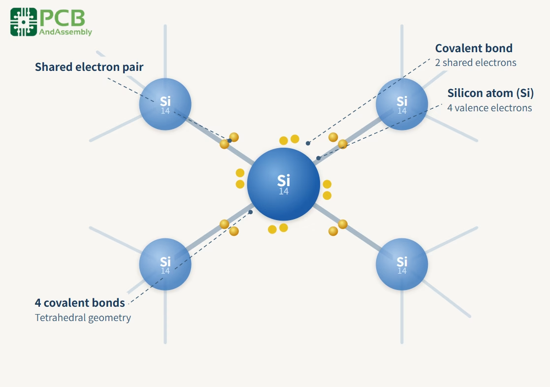
From the smartphone in your pocket to the advanced chips powering artificial intelligence, semiconductors are the unseen heroes of modern electronics. These fascinating materials possess electrical conductivity that falls between that of a conductor (like copper) and an insulator (like glass). This unique property allows us to precisely control electrical current, making complex electronic devices possible. The most common semiconductor materials are silicon (Si) and germanium (Ge), both of which have four valence electrons in their outermost shell, enabling them to form stable covalent bonds in a crystal lattice.
1.2 The Band Theory of Solids
To understand why semiconductors are so special, it helps to consider the band theory of solids. In conductors such as metals, the valence band and conduction band overlap, so electrons flow freely at all times. In insulators, the energy gap — known as the bandgap — between the two bands is so large that electrons practically never cross it. Semiconductors occupy the middle ground: their bandgap is small enough that electrons can be pushed into the conduction band by heat, light, or — crucially — chemical doping.
1.3 Intrinsic vs. Extrinsic Semiconductors
Semiconductors are broadly categorized into two types: intrinsic and extrinsic. Intrinsic semiconductors are pure materials, like perfectly crystalline silicon, where the number of free electrons and “holes” (electron vacancies) is equal. While pure semiconductors have some utility, their conductivity is too low for most practical electronic applications. To enhance and control their conductivity, we introduce a process called doping.
Doping involves adding tiny, controlled amounts of impurity atoms to an intrinsic semiconductor. This process transforms a pure material into an extrinsic semiconductor, dramatically altering its electrical properties. Depending on the type of impurity added, we create either P-type or N-type semiconductors, each with distinct electrical characteristics and crucial roles in the functionality of virtually every electronic component. Understanding these two fundamental types is key to grasping how modern technology works.
2. P-Type Semiconductors: Harnessing Positive Holes
A P-type semiconductor is an extrinsic semiconductor created by doping a pure (intrinsic) semiconductor with trivalent impurities. Trivalent elements are those from Group III of the periodic table, possessing three valence electrons. Common examples include boron (B), aluminum (Al), and gallium (Ga). When these impurity atoms are introduced into a silicon crystal lattice, they attempt to form covalent bonds with the surrounding silicon atoms.
2.1 The Doping Process
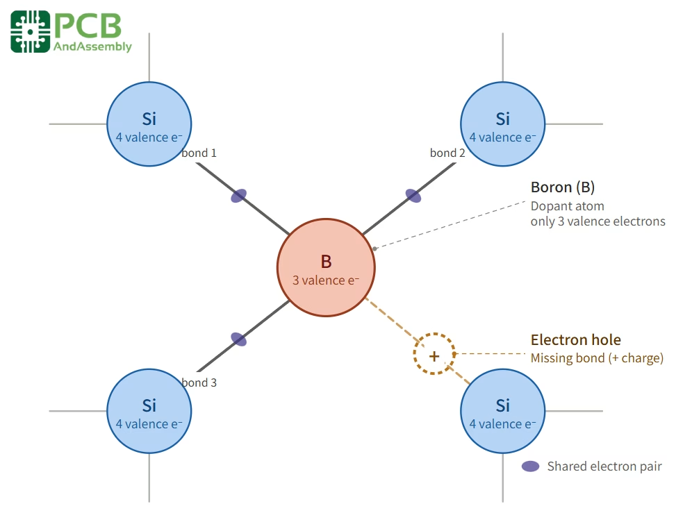
Since each silicon atom has four valence electrons and the trivalent impurity atom only has three, there is a “missing” electron in one of the bonds. This electron deficiency creates a vacancy known as a “hole.” These holes behave as if they carry a positive charge and are readily available to accept an electron from a neighboring atom. In a P-type material, these holes are the majority charge carriers, meaning they are primarily responsible for carrying electrical current. The trivalent impurity atoms are therefore called “acceptor” impurities because they “accept” electrons, thereby generating holes.
When an electric field is applied, electrons from adjacent covalent bonds jump into these holes, effectively causing the holes to move in the opposite direction to the electron flow. This movement of holes constitutes the electric current. While electrons are still present in P-type material, their concentration is significantly lower than that of holes, making them the minority charge carriers. The higher the concentration of acceptor impurities, the greater the density of holes, and consequently, the higher the conductivity of the P-type semiconductor.
2.2 Band Structure and Fermi Level
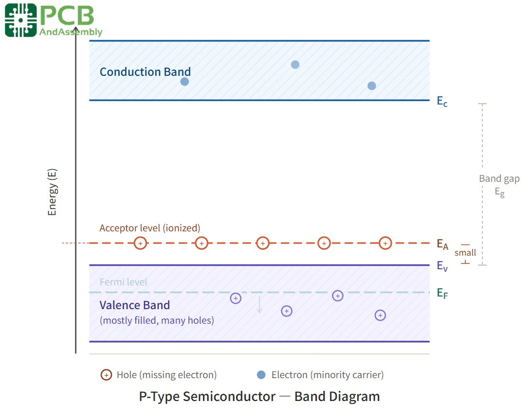
In terms of energy band structure, the acceptor impurities create energy levels just above the valence band. This causes the Fermi level — the energy level at which an electron has a 50% probability of occupation — to shift closer to the valence band than in an intrinsic semiconductor. The small energy difference between the valence band and these acceptor energy levels means that electrons can easily transition to the acceptor levels, leaving behind holes in the valence band. This is why P-type materials are rich in holes and have a Fermi level positioned near the bottom of the bandgap.
2.3 Electrical Conductivity
In P-type semiconductors, conductivity is dominated by the movement of holes under an applied electric field. Holes migrate from regions of high potential to low potential, constituting the current flow. Both temperature and doping concentration affect conductivity: raising the temperature increases thermal generation of electron-hole pairs, boosting conductivity; raising the doping concentration directly increases the number of acceptor-generated holes, also increasing conductivity. However, hole mobility is inherently lower than electron mobility, since holes “hop” between bonds rather than moving as free particles.
2.4 Applications of P-Type Semiconductors
P-type semiconductors are essential to a wide range of electronic devices:
- PN junction diodes: The P-type side provides the positive terminal, enabling current rectification.
- PNP transistors: P-type regions sandwich an N-type base, allowing the device to amplify or switch current.
- Photodiodes and solar cells: Illumination generates electron-hole pairs, separated by the junction electric field.
- CMOS circuits: P-type MOSFETs (PMOS) work alongside N-type MOSFETs in complementary logic gates.
3. N-Type Semiconductors: Leveraging Negative Electrons
In contrast, an N-type semiconductor is formed by doping an intrinsic semiconductor with pentavalent impurities. Pentavalent elements belong to Group V of the periodic table, meaning they have five valence electrons. Typical examples include phosphorus (P), arsenic (As), and antimony (Sb). When these atoms are incorporated into a silicon crystal lattice, four of their five valence electrons form covalent bonds with the surrounding silicon atoms.
3.1 The Doping Process
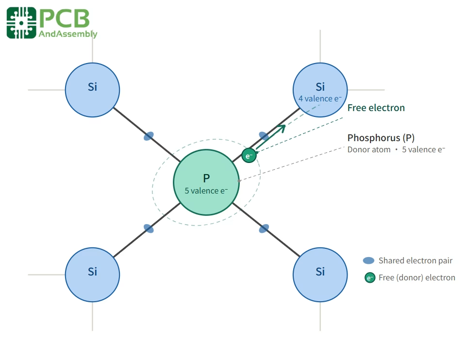
The fifth valence electron of the pentavalent dopant is not needed for bonding and remains very loosely bound to the impurity atom. This excess electron requires very little energy — far less than the bandgap energy — to break free and become a conduction electron that can move through the crystal lattice. In an N-type material, these free electrons are the majority charge carriers, responsible for most of the electrical current flow. The pentavalent impurity atoms are called “donor” impurities because they “donate” an extra electron to the semiconductor.
When an electric field is applied, these free electrons migrate from high-potential to low-potential regions, producing a current. While holes are still present due to thermal excitation, their concentration is far lower than that of the free electrons, making them the minority charge carriers. The greater the concentration of donor impurities, the higher the density of free electrons, leading to increased conductivity of the N-type semiconductor.
3.2 Band Structure and Fermi Level
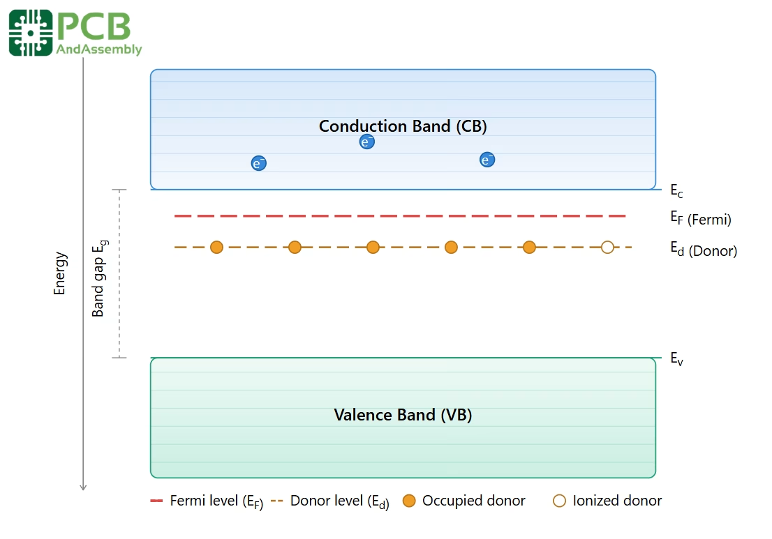
In N-type semiconductors, donor impurities create energy levels just below the conduction band. This shifts the Fermi level upward, closer to the conduction band. Because the energy gap between these donor levels and the conduction band is very small, electrons can easily transition into the conduction band without needing to cross the full bandgap. This abundance of near-conduction-band electrons is what gives N-type materials their high free electron concentration and explains why the Fermi level is positioned near the top of the bandgap.
3.3 Electrical Conductivity
Free electrons in N-type semiconductors move very efficiently under an electric field, giving these materials high conductivity. Because electrons are the primary current carriers and possess higher mobility than holes (they travel as free particles, not by hopping between bonds), N-type regions typically exhibit somewhat higher conductivity than equivalently doped P-type regions. As with P-type, both temperature and doping concentration influence conductivity: higher temperature increases thermal carrier generation, while higher doping concentration directly increases the donor electron supply.
3.4 Applications of N-Type Semiconductors
N-type semiconductors are equally fundamental to modern electronics:
- NPN transistors: N-type emitter and collector regions surround a P-type base, forming a versatile amplifier and switch.
- N-type MOSFETs (NMOS): Widely used in digital logic and power electronics for their high carrier mobility and switching speed.
- Voltage regulators and rectifier diodes: N-type material forms the cathode of diodes used to control and convert electrical power.
- Solar cells: N-type silicon serves as the electron-collecting layer, paired with P-type to form the photovoltaic junction.
4. The Core Differences: P-Type vs. N-Type
While both P-type and N-type semiconductors are extrinsic materials, their fundamental differences in doping elements, charge carrier types, and band structures make them distinct and complementary. The table below provides a comprehensive side-by-side comparison:
| Feature | P-Type Semiconductor | N-Type Semiconductor |
| Doping Element | Trivalent (Group III): Boron (B), Aluminum (Al), Gallium (Ga) | Pentavalent (Group V): Phosphorus (P), Arsenic (As), Antimony (Sb) |
| Impurity Type | Acceptor impurities (accept electrons, create holes) | Donor impurities (donate extra electrons) |
| Majority Charge Carriers | Holes (positively charged vacancies) | Free electrons (negatively charged particles) |
| Minority Charge Carriers | Electrons | Holes |
| Conduction Mechanism | Movement of holes through the lattice | Movement of free electrons through the lattice |
| Fermi Level Position | Closer to the valence band | Closer to the conduction band |
| Carrier Mobility | Lower (holes “hop” between bonds) | Higher (electrons move freely) |
| Overall Charge | Electrically neutral | Electrically neutral |
| Role in Circuits | Positive terminal; used in PNP transistors, photodiodes | Negative terminal; used in NPN transistors, MOSFETs |
A key nuance worth emphasizing is the overall charge neutrality of both types. Although P-type material has an abundance of positive holes and N-type material has an abundance of negative electrons, both are electrically neutral overall. This is because the impurity ions are fixed in the crystal lattice and carry a charge that exactly cancels the mobile carriers they produce. For example, in N-type silicon, each donor ion becomes a fixed positive ion after donating its electron — perfectly balancing the free negative electron it contributed.
Another important distinction is carrier mobility. Electrons in N-type semiconductors can move freely as independent particles through the conduction band, while holes in P-type semiconductors “move” by a successive exchange of electrons between adjacent bonds — a slower, hopping mechanism. As a result, at equal doping levels, N-type regions generally conduct electricity slightly more efficiently than P-type regions.
5. The PN Junction
While P-type and N-type semiconductors are powerful on their own, their true potential is unleashed when they are joined together to form a PN junction. This junction is the fundamental building block of almost all modern electronic devices. Understanding the PN junction requires examining what happens at the interface between the two materials.
5.1 Formation of the Depletion Region
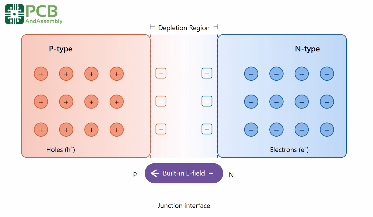
When P-type and N-type materials are brought into contact, a critical process called carrier diffusion occurs immediately. Free electrons from the N-type region diffuse across the junction into the P-type region (where electron concentration is lower), while holes from the P-type region diffuse in the opposite direction into the N-type region. As this exchange takes place:
- Electrons from the N-side fill holes near the junction on the P-side, creating fixed negative ions in the P-type region.
- The departure of electrons from near the junction on the N-side leaves behind fixed positive donor ions.
- This creates a narrow zone — the depletion region — devoid of mobile charge carriers.
- The separated fixed charges generate an internal electric field (built-in potential) that opposes further diffusion, eventually reaching equilibrium.
The depletion region acts as an insulating barrier at equilibrium. Its width and the strength of the internal electric field depend on the doping concentrations on each side.
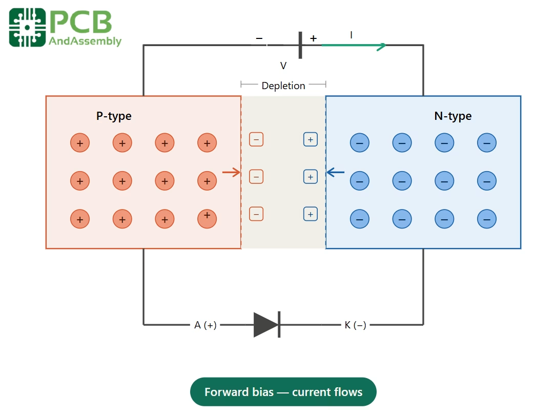
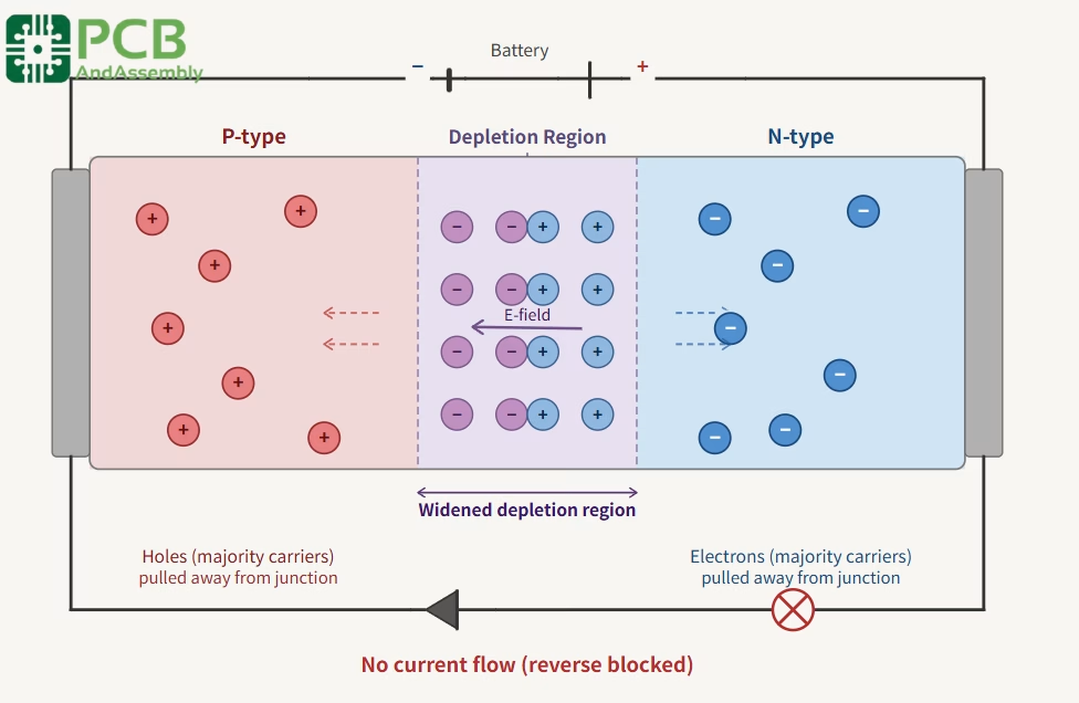
5.2 Forward and Reverse Bias
The behavior of a PN junction changes dramatically depending on how an external voltage is applied:
Forward bias: When the positive terminal of a power supply is connected to the P-type side and the negative terminal to the N-type side, the applied voltage counteracts the internal electric field, narrowing the depletion region. Once the applied voltage exceeds the built-in potential (approximately 0.7 V for silicon), charge carriers flow freely across the junction, and current passes readily.
Reverse bias: When the connections are reversed — positive to N-type, negative to P-type — the applied voltage reinforces the internal electric field, widening the depletion region. This prevents majority carriers from crossing, and only a tiny leakage current flows. If the reverse voltage is increased sufficiently, breakdown occurs (exploited deliberately in Zener diodes) and current surges through the junction.
5.3 Synergistic Effect
The PN junction operates because P-type and N-type regions collaborate through diffusion and field effects. The P-type side supplies holes that can receive electrons under forward bias, while the N-type side supplies electrons that can recombine with those holes. This cooperative behavior is what gives the junction its rectifying properties — and makes it the cornerstone of modern electronics.
Need PCB Manufacturing or Assembly?
Get a free quote within 24 hours. We specialize in prototype-to-production PCB/PCBA for hardware teams worldwide.
6. Key Applications of PN Junctions
6.1 Diodes: The One-Way Valve
The simplest and most direct application of a PN junction is the diode. Acting like a one-way valve for electric current, a diode permits current to flow easily in forward bias and blocks it under reverse bias. This rectifying property is essential for converting alternating current (AC) to direct current (DC) — a step required to power virtually all electronic devices from household appliances to computing equipment.
6.2 Transistors: Amplifiers and Switches
More complex structures such as transistors are formed by combining multiple PN junctions into NPN or PNP configurations. Transistors serve two vital roles: as switches, they turn current on or off to encode binary logic; as amplifiers, they boost weak signals for use in communications, audio systems, and sensors. The speed and reliability of transistor switching is what makes modern computing possible.
6.3 Integrated Circuits: The Brains of Devices
Thousands, millions, or even billions of PN junctions — configured as diodes and transistors — can be fabricated onto a single tiny silicon chip to create an integrated circuit (IC). ICs are the brains of modern electronics, performing complex calculations, storing data, and managing operations in everything from microprocessors to memory chips. The miniaturization enabled by controlled P-type and N-type doping has driven the extraordinary pace of technological progress over the past half-century.
6.4 Solar Cells: Harnessing Light
PN junctions also excel at energy conversion. In a solar cell, incoming photons excite electrons in the semiconductor, generating electron-hole pairs. The built-in electric field of the depletion region separates these carriers — electrons are swept toward the N-type side and holes toward the P-type side — producing a usable electric current. This direct conversion of light to electricity is the basis of all photovoltaic technology and a cornerstone of modern renewable energy.
6.5 LEDs: Emitting Light
In a light-emitting diode (LED), the process runs in reverse from a solar cell. Under forward bias, electrons and holes are injected into the junction from opposite sides and recombine. The energy released during recombination is emitted as a photon of light. By selecting semiconductor materials with specific bandgap energies, engineers can produce LEDs that emit virtually any visible color, as well as infrared and ultraviolet light — enabling applications from display backlighting to fiber-optic communications.
7. Frequently Asked Questions
Q1: Are P-type and N-type semiconductors positively or negatively charged overall?
Both are electrically neutral. Although P-type material contains an abundance of positive holes and N-type material contains an abundance of free electrons, the impurity ions fixed in the crystal lattice carry an equal and opposite charge. For instance, each donor ion in N-type silicon becomes a fixed positive ion that exactly cancels the mobile electron it donated.
Q2: What is the primary difference between intrinsic and extrinsic semiconductors?
Intrinsic semiconductors are pure materials (e.g., undoped silicon) whose conductivity is determined entirely by thermal excitation, resulting in equal numbers of electrons and holes. Extrinsic semiconductors are doped with impurities to increase conductivity and to make either electrons (N-type) or holes (P-type) the dominant carriers, enabling precise engineering of electrical behavior.
Q3: Why are silicon and germanium the most common semiconductor base materials?
Both silicon (Si) and germanium (Ge) are Group IV elements with four valence electrons, forming stable and symmetric covalent lattice structures. This tetrahedral bonding makes them ideal hosts for doping: substituting a Group III or Group V atom fits naturally into the lattice, creating predictable numbers of holes or electrons. Silicon has largely superseded germanium for most applications due to its wider bandgap (better high-temperature performance), its abundance, and the exceptional quality of its native oxide (SiO₂), which is critical for MOSFET gate insulation.
Q4: Can doping concentration be changed after fabrication?
In general, no — once a semiconductor device is fabricated, its doping profile is fixed. However, during manufacturing, engineers use techniques such as ion implantation and diffusion to build up complex doping profiles within a single chip, creating precisely defined regions of P-type and N-type material separated by nanometers. This is how modern transistors with feature sizes below 5 nm are built.
Q5: Why do N-type semiconductors typically have slightly higher conductivity than P-type at equal doping levels?
Electron mobility in silicon (approximately 1,400 cm²/V·s) is roughly 2–3 times higher than hole mobility (approximately 450 cm²/V·s). Electrons move freely through the conduction band, while holes advance by a sequence of electron transfers between adjacent bonds — a slower, indirect process. At equal doping concentrations, the higher mobility of electrons gives N-type regions a conductivity advantage.
8. Summary
N-type and P-type semiconductors are the backbone of the electronic age. Through the precise process of doping, intrinsic semiconductors like silicon are transformed into extrinsic materials with tailored electrical properties. P-type semiconductors, doped with trivalent (Group III) impurities, rely on “holes” as their majority charge carriers; their Fermi level resides near the valence band. N-type semiconductors, doped with pentavalent (Group V) impurities, utilize free electrons as their majority carriers; their Fermi level sits near the conduction band.
When placed in contact, these two materials form a PN junction — featuring a depletion region, a built-in electric field, and the ability to selectively conduct under forward bias while blocking under reverse bias. This simple yet profound interface is the foundation of diodes, transistors, solar cells, LEDs, and integrated circuits, underpinning nearly every electronic device in use today.
A clear grasp of P-type and N-type semiconductors, their differences, and their synergy in PN junctions is essential for anyone seeking to understand modern electronics — from the principles of circuit design to the physics driving the next generation of computing and energy technologies.
Key Takeaways
- P-type semiconductors use trivalent (Group III) impurities — boron, aluminum, gallium — to create “holes” as majority charge carriers.
- N-type semiconductors use pentavalent (Group V) impurities — phosphorus, arsenic, antimony — to create free electrons as majority charge carriers.
- Both P-type and N-type semiconductors are electrically neutral; their conductivity comes from mobile charge carriers, not from net charge.
- The Fermi level in P-type material is closer to the valence band; in N-type material, it is closer to the conduction band.
- Electrons have higher mobility (~1,400 cm²/V·s) than holes (~450 cm²/V·s), so N-type regions typically conduct more efficiently at equal doping concentrations.
- Combining P-type and N-type materials forms a PN junction — the essential building block of diodes, transistors, LEDs, solar cells, and integrated circuits.
- Forward bias narrows the depletion region and allows current flow; reverse bias widens it and blocks current.

Get Quote Free