Preventing Void Issues in PCB Manufacturing
Get Your PCB Quote!

Table of Contents
Table of Contents
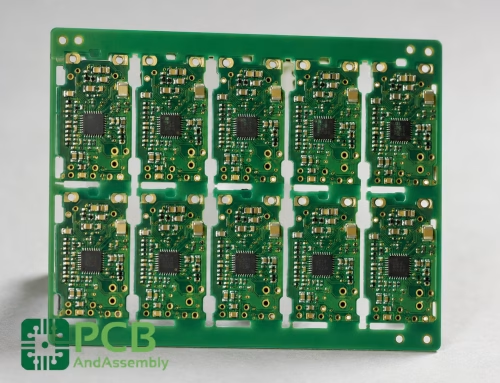
At Pcbandassembly, we produce a wide range of printed circuit boards (PCBs). To prevent frequent quality problems, we must use extreme caution when using the various instruments and procedures during the manufacturing process. These issues include cold solder joints, brittle solder joints, and voids. A void is a gap where there is insufficient material somewhere in the PCB. Void issues are very important and can result in a scrapped PCB if not handled properly. Understanding void concerns and other challenges brought on by voids is so essential.
1. What are PCB Voids?
Anywhere in the PCB’s non-plated region, voids can form. This may be in a solder joint, the barrel of a hole, or the wall of a hole bored beneath the plating. Voids often disrupt electrical continuity within a circuit, causing the PCB to fail.
2. PCB Void Types
There are two main common types of voids in the PCB manufacturing process, and it is important for our customers to understand the measures we take to avoid voids.
1) Plating Voids
There may be plating voids if the inner wall of the PCB hole is not entirely covered by the plating during the electroless copper plating process. Such voids are usually caused by drilling when creating a through hole. When drilling, a dull drill bit will leave imperfections on the wall rather than creating a smooth surface.
A dull drill bit typically creates a rough hole wall with numerous flaws. Many areas on the hole wall may remain non-plated when copper is added during the electroless copper plating process because the copper may not be able to reach all the rough depressions and gaps. Debris may also get stuck in the hole as a result of drilling. This material frequently occurs when a worker removes the drill bit without cleaning the hole thoroughly.
When debris or other impurities become stuck in a plated hole, the copper plating may cover the debris or contaminants for a short time. Later, as the debris breaks off the hole walls, the copper that covered it may be removed, leaving a void. Another way that plating voids can form is when there are bubbles on the hole walls. During the plating process, the bubbles prevent copper from being deposited beneath them, thus forming a void.
How to Prevent Plating Voids
One technique to avoid voids when drilling is to use sharp drill bits. Operators must keep track of discarded or sharpened drill bits based on drilling speed, feed, and number of hits. They have to use the right holds and cleaning techniques for every drill hole. Monitoring the agitation of the plating solution in the tank can also help reduce and eliminate plating voids. For example, using line vibration and tilting the plating rack can release trapped air during the electroless plating process. We never waste drill bits and refrain from using them after a predetermined number of uses. We also used a desmear procedure to remove any foreign objects that had been created during the drilling operation.
2) Solder Voids
Solder voids occur when an operator uses an insufficient amount of solder paste. Additionally, there may be air pockets in the solder paste that are unable to escape when the paste is not heated sufficiently. The board becomes worthless in both of these voiding scenarios, and the manufacturer might be forced to discard it.
Solder voids can also occur from voids within the solder joints. Many factors can cause this problem, including setting the preheat temperature too low, which prevents the solvents in the flux from fully evaporating. Other factors include high flux content, oxidation of the solder paste, or using low-quality solder paste. The design of the PCB and its stencil may also, in some cases, make it more vulnerable to voids.
Typical Causes of Solder Voids
√ Insufficient preheat temperature during reflow
√ Out gassing of organic brighteners
√ Impure or poor quality flux in solder paste
√ Presence of water or moisture on PCB surface or in solder paste
√ Excessive oxide on silver plating
√ Contamination of solder mask on copper
How to Prevent Solder Voids
Compared to plating voids, which are the two main forms of voids, solder voids are usually easier to prevent. Extending the warm-up period, limiting the use of low-quality or expired solder paste, and altering the stencil design are all efficient ways to lower the chance of solder voids.
3) Micro Voids
Another kind of solder void is called a micro void, which occurs when a lot of tiny holes form at the solder joint’s interface. Typically, fewer than 40 microns in diameter, micro voids are found directly above the inter-metallic connection layer that connects the solder paste’s tin to the circuit board’s copper.
Like solder voids, micro voids can be troublesome when they are numerous enough and reduce the cross-sectional area of a joint. In severe situations, thousands of micro voids may result in a joint’s physical and electrical failure. The existence of micro voids could not have been detected previously. Micro voids can now be found using high-resolution X-ray examination techniques.
Causes of Micro Void Formation
√ Use of Lead-Free Solder
One of the causes of the rise of micro voids is the growing usage of lead-free solder. Compared with lead-containing solder, the lead-free solder reflow process requires higher temperatures. This increases the possibility of temperature variations across the board. Furthermore, micro void formation may also result from variations in flux chemistry and surface tension among lead-free solder brands.
√ Contamination of Board Surface
With the transition to lead-free solder, manufacturers are also offering new surface finishes for PCB boards. For instance, a common surface finish is immersion silver. Micro gaps can, however, also be caused by problems with process control, such as contamination of the board surface from oil, developer foam, tin resistance, and sublimated solder mask volatile coatings.
√ The Copper Pad Surface is Too Rough
Another reason for micro voids is that the copper pad surface is too rough. Just as a solder joint may have multiple micro voids, resulting in a larger solder void, small bubbles on a rough copper surface can also produce micro voids. Copper surfaces can get rough from a number of different techniques. Changes in current density during electroplating can produce a rough surface by changing the deposit.
The copper surface may also be negatively impacted by tin stripping or solder mask preparation before surface treatment. Although micro-etching and cleaning chemicals are used in surface treatment procedures, they are not strong enough to remove dirt or rough copper surfaces because they are very weak compounds.
√ Silver Finish Reworking
The copper surface may also suffer if the silver coating is reworked. This happens when operators put the PC through the plating tank several times in order to rework the silver finish. This affects the integrity of the silver deposit and the copper surface.
How to Prevent Micro Voids
Although micro gaps are a result of extremely thick silver coatings, an immersion silver coating cannot be significantly thinner. For instance, plating thicknesses less than 0.13 microns may cause potential loss of contact functionality, increased tarnishing, and increased copper migration through the pores. Micro void formation can be minimized by decreasing the thickness of the immersion silver coating while maintaining it above the lower limit.
However, if the other processes are not maintained and developed, it is of little use to pay great attention to the quality of immersion silver. Tin and organic residues must not be present on the copper surface. The copper surface needs to be relatively smooth. Copper that has undergone micro-etching before silver deposition must have a consistent, clean surface.
Rework must be limited according to the supplier’s recommendations. Excessive rework will produce a rough silver surface that will perform the same as a thick silver deposit. After silver deposition, ionic residues on the board must be controlled by rinsing, careful handling, and packaging.
During assembly, moderate preheat temperatures and slow ramp rates can be used to prevent the formation of micro voids. In addition, the use of low-voiding fluxes and better control of solder paste storage may be necessary to effectively prevent micro voids.
3. Summary
PCB rejection due to voids can quickly make the PCB manufacturing process expensive. According to Pcbandassembly, taking a few precautions and paying special attention to detail is enough to prevent the formation of PCB voids. To prevent voids and guarantee the high caliber of the circuit boards, this calls for the use of premium sharp drill bits, improved cleaning techniques, and thorough testing.

Get Quote Free