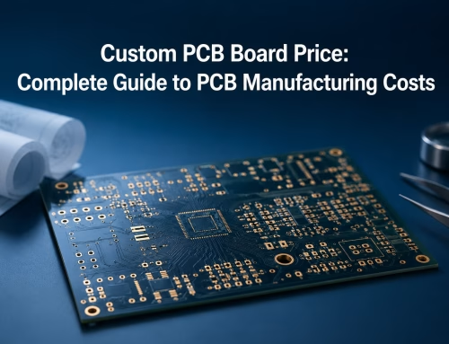
How Much Does PCB Manufacturing Cost in 2026?
The cost of PCB manufacturing in 2026 is shaped by a convergence of pressures unlike any previous market cycle. Where earlier years saw isolated spikes in copper or gold prices, the current environment features simultaneous cost escalation across every major layer of the electronics bill of materials (BOM) — substrates, laminates, memory, and active components — each driven by independent structural causes with different resolution timelines.
Get Your PCB Quote!
Table of Contents
- 1. The 2026 BOM Crisis at a Glance
- 2. The Material and Substrate Cost Crisis
- 3. Bare Board Fabrication Economics: Layers, Vias, and Features
- 4. PCB Cost Estimation by Layer and Board Type
- 5. Fabrication Facility Economics: Why Volume Matters
- 6. Strategic DFM Rules to Mitigate 2026 Cost Risks
- 7. Procurement Strategy in a Full BOM Crisis
- 8. When Will the Pressure Ease? A 2026–2027 Outlook
- 9. Frequently Asked Questions
- How much does an HDI board typically cost in 2026?
- Summary
Industry data shows that net BOM costs for high-density systems have surged 25% to 40% compared to the latter half of 2025. Total cloud service provider (CSP) capital expenditure is forecast to exceed $60 billion in 2026 — a 40% year-on-year increase — consuming a disproportionate share of global manufacturing capacity and raw materials. Understanding where costs originate, and how design choices amplify or mitigate them, is essential for any engineering or procurement team working in this environment.
1. The 2026 BOM Crisis at a Glance
The 2026 cost environment differs from previous cycles because the pressure points are structurally independent. They have different causes, different timelines, and different potential resolution paths — which makes managing them simultaneously far more difficult than handling a single-material crisis.
Key cost drivers as of mid-2026:
| BOM Category | Cost Change (Q3 2025 → Q2 2026) | Lead Time Change | Risk Level |
| PCB bare board (standard) | +15–25% | 4–8 wks (was 2–4) | Moderate |
| High-Tg / ENIG PCB | +30–45% | 6–10 wks; quota risk | High |
| DRAM (standard DDR) | +90–110% | 16–24 wks; allocation | Critical |
| MCUs (TI, Infineon, NXP) | +15–85% | 20–40 wks | Critical |
| Nexperia discretes | Supply frozen | No timeline | Severe — redesign required |
*Cost changes measured against equivalent H2 2025 designs.
The practical implication: a design costed in Q3 2025 for production in Q2–Q3 2026 may face a total BOM increase of 30–60%, depending on the component mix. Designs incorporating DRAM and affected MCU families are likely to land at the upper end of that range.
Need PCB Manufacturing or Assembly?
Get a free quote within 24 hours. We specialize in prototype-to-production PCB/PCBA for hardware teams worldwide.
2. The Material and Substrate Cost Crisis
The Copper and Fiberglass Double Bottleneck
Copper prices hovering near historic highs of over $13,300 per metric ton represent a major burden on PCB fabrication. However, the more severe and less-discussed constraint is the fiberglass dielectric base of Copper Clad Laminates (CCL).
Low-CTE (coefficient of thermal expansion) glass fiber fabric — the foundational substrate for high-speed, high-frequency PCBs — is currently in a genuine structural shortage. This bottleneck is entirely independent of copper pricing: even if copper prices moderated tomorrow, the fiberglass shortage would continue to constrain CCL supply. The consequences include:
- CCL costs up to 45% higher across all grades
- Lead times extending to 6 months for advanced laminate grades
- Quota systems imposed by major CCL suppliers
- Allocation pressure cascading into standard-grade FR-4 as manufacturers prioritize high-margin high-end laminates
Ramping low-CTE glass fiber capacity is capital-intensive and requires long qualification cycles, making this the constraint with the longest resolution timeline — potentially extending well into 2027.
High-Frequency Laminate Material Tiers
For high-speed signal transmission, standard FR-4 introduces unacceptable dielectric loss. At 224 Gbps signaling rates, M7-grade ultra-low-loss laminate is mandatory. At 448 Gbps+ for next-generation platforms, M9/M10 grades are required. The following table details performance, availability, and cost for key substrate materials in 2026:
| Material Grade | Df @ 10 GHz | 2026 Lead Time | Cost vs FR-4 | Primary Application |
| Standard FR-4 | 0.015–0.020 | 2–3 weeks | 1.0× | Consumer electronics, basic industrial |
| High-Tg FR-4 | 0.012–0.014 | 3–5 weeks | 1.3–1.5× | Automotive ECUs, multilayer industrial |
| Megtron 6 (M6) | 0.004 | 8–12 weeks | 4.5–5.5× | 100G Ethernet, enterprise storage |
| Megtron 7 (M7) | 0.002 | 16–20 weeks (restricted) | 6.0–9.0× | 224 Gbps signaling, AI server backplanes |
| Megtron 9/10 (M9/M10) | < 0.001 | 24+ weeks (allocation) | 15–20× | 448 Gbps+ cards, optical transport |
| Rogers 4350B | 0.0037 | 12–16 weeks | 8.0–10.0× | RF power amplifiers, radar front-ends |
Designers should note that specifying M7–M10 materials today may mean waiting six months or longer for substrate availability — a timeline that can invalidate standard production planning assumptions.
3. Bare Board Fabrication Economics: Layers, Vias, and Features
The Non-Linear Cost of Layer Counts
Fabrication complexity does not scale linearly with layer count. Each step up in layers introduces additional lamination cycles, tighter registration tolerances, and higher cumulative risk of layer misalignment — and if any internal layer is defective after lamination, the entire multilayer panel is scrapped.
Key process differences by stackup:
- 2-layer: Single core, single drill-plate-etch cycle — the most economical path.
- 4-layer: Adds prepreg sheets and external copper foil, bonded under hydraulic vacuum press.
- 8–12 layer: Each additional pair of internal layers adds processing steps, registration requirements, and yield loss exposure.
- 24+ layer: Manufacturing complexity compounds significantly; used almost exclusively for advanced server and networking applications.
Via Architecture and Its Cost Impact
The via implementation strategy chosen for a design is one of the most significant levers on bare board pricing. The table below summarizes cost multipliers relative to a standard double-sided mechanically-drilled PCB:
| Design Feature | Baseline | Advanced Spec | Cost Multiplier | Technical Driver |
| Via Structure | Through-Hole (Mechanical) | 1+N+1 HDI (Laser Microvias) | 1.5×–2.0× | Laser drilling, copper-fill, two lam. cycles |
| Via Structure | Through-Hole (Mechanical) | Any-Layer HDI (ELIC) | 3.0×–4.5× | Every layer pair: independent lam., drill, plate |
| Copper Weight | 1 oz (35 µm) | 3 oz (105 µm) Heavy Copper | 1.3×–1.6× | Higher copper volume, longer etch times |
| Trace & Space Width | > 5 mils (0.127 mm) | < 3 mils (0.075 mm) | 1.25×–1.4× | Requires LDI imaging, cleanroom controls |
| Impedance Control | No control | Controlled (±10% tolerance) | 1.1×–1.15× | Strict dielectric tolerances + TDR testing |
HDI designs requiring blind or buried vias cannot be fabricated on standard through-hole lines. Sequential lamination is required: the fabricator laminates the inner core, drills and plates buried vias, adds outer layers, then drills and plates outer vias. When via diameters fall below 0.15 mm, laser drilling replaces mechanical drilling — adding specialized desmear and copper-fill plating steps.
Surface Finishes: Cost, Performance, and When Each Makes Sense
Surface finishes protect exposed copper pads from oxidation and ensure reliable solder joint formation. Selection should be driven by component requirements, not default habit:
| Surface Finish | Surface Quality | Cost Level | Best For | Key Risk |
| Lead-Free HASL | Uneven | Low (baseline) | Through-hole, simple SMT | Bridging on fine-pitch components |
| ENIG | Flat | Moderate (+20–35%) | Fine-pitch BGAs, 0201 passives, QFNs | ‘Black pad’ corrosion risk |
| ENEPIG | Flat + wire-bondable | High (+35–50%) | Wire bonding, high-reliability | Highest cost option |
Industry data indicates that upgrading from Lead-Free HASL to ENEPIG on a large double-sided board can increase bare board fabrication cost by 20–35%, even when the electrical design is simple. For designs using fine-pitch BGAs, QFNs, or 0201 passives, the flat surface of ENIG or ENEPIG is not optional — it is a yield requirement.
4. PCB Cost Estimation by Layer and Board Type
The following table presents estimated unit cost ranges for standard 100 mm × 100 mm boards across various layer configurations and material types in 2026, at moderate-to-high production volumes (1,000+ units):
| PCB Type | Substrate | Unit Cost (1k vol.) | Prototype (5–10 pcs) | Key Cost Drivers |
| 1-Layer / Single-Sided | Standard FR-4 | $0.50–$3.00 | $25–$50 | Punching vs. routing, tooling fees |
| 2-Layer / Double-Sided | Standard FR-4 / High-Tg | $2.00–$12.00 | $40–$80 | Hole count, surface finish |
| 4-Layer Multilayer | High-Tg FR-4 | $12.00–$35.00 | $150–$250 | Lamination cycles, copper thickness |
| 8-Layer Multilayer | High-Tg FR-4 / M6 | $30.00–$75.00 | $350–$600 | Impedance control, layer registration |
| HDI (Laser Microvias) | Low-loss (M6/M7/Rogers) | $40.00–$150.00 | $800–$1,500 | Laser drill, stacked via alignment |
| Rigid-Flex (4–6 Layer) | Polyimide + FR-4 Hybrid | $100.00–$400.00 | $1,200–$2,500 | Manual prep, adhesive layers, routing |
Notes on Specific Board Types
Single and Double-Layer Boards
These remain highly cost-effective. Key variables are physical dimension, total hole count, and surface finish. Upgrading from Lead-Free HASL to ENIG on a large double-sided board can double the base fabrication cost, even on a simple design.
Multilayer and HDI Boards
Transitioning to 4-layer introduces internal ground and power planes, significantly increasing process steps. HDI designs command a further premium due to laser microvia drilling, copper-filled plating, sequential lamination cycles, and the requirement for low-loss laminates — all compounding the raw material expense.
Rigid-Flex Boards
Rigid-flex boards combine rigid laminate layers with flexible polyimide cores, enabling designs that fold into tight mechanical enclosures without internal wire harnesses. The tradeoff is significant manufacturing complexity:
- Specialized adhesives and precise hydraulic press profiles are required to accommodate the differing CTE characteristics of polyimide and glass-epoxy.
- Manual labor for flexible material preparation and board outline routing is substantial.
- Despite the high per-unit cost ($100–$400+), rigid-flex can reduce overall system cost by eliminating board-to-board connectors and improving vibration reliability.
About PCBAndAssembly
Time is money in your projects – and PCBAndAssembly gets it. PCBAndAssembly is a PCB assembly company that delivers fast, flawless results every time. Our comprehensive PCB assembly services include expert engineering support at every step, ensuring top quality in every board. As a leading PCB assembly manufacturer, we provide a one-stop solution that streamlines your supply chain. Partner with our advanced PCB prototype factory for quick turnarounds and superior results you can trust.
5. Fabrication Facility Economics: Why Volume Matters
Fixed Monthly Overhead
A typical mid-to-high capability PCB fabrication facility in 2026 carries approximately $122,000 in fixed monthly operating expenses before processing any material. These fixed costs include:
- Equipment depreciation — CNC drills, laser direct imaging (LDI) systems, AOI machines, and automated plating lines require continuous capital depreciation.
- Environmental compliance — wastewater treatment for copper-laden etch effluents and chemical scrubbing systems must run continuously.
- Facility maintenance — Class 1000 and Class 100 cleanrooms for photolithography require 24/7 temperature, humidity, and particulate control.
- Direct labor — skilled CAM engineers, wet chemistry process technicians, and QA inspectors represent a largely fixed labor cost.
These fixed costs establish a pricing floor for low-volume orders. Fabricators recover them through tooling, engineering setup, and photoplotting fees on prototype and small-batch runs.
The Volume-Cost Relationship
As order volume increases, fixed setup costs are amortized across more units. Meaningful economies of scale typically begin at 500–1,000 units, at which point fixed tooling represents a negligible fraction of per-board cost. Variable costs — raw laminates, copper foil, process chemicals, assembly labor — then become the primary driver.
Panelization efficiency is an often-overlooked variable cost lever. Boards are fabricated on standard production panels (typically 18″ × 24″ or 12″ × 18″). A design that utilizes only 60% of panel area means the buyer is paying for 40% that ends up as scrap. Minor dimensional adjustments — sometimes as small as 2 mm — can shift a design from 8 boards per panel to 12, directly reducing per-board substrate cost.
6. Strategic DFM Rules to Mitigate 2026 Cost Risks
In the current high-cost environment, Design for Manufacturability (DFM) cannot be treated as a post-layout checklist. These rules should be integrated during the layout phase:
Rule 1: Standardize Geometry Specifications
Trace and space widths below 3 mils or via drill diameters smaller than 0.15 mm push the PCB into the high-precision category, requiring advanced imaging and drilling systems. Unless high-density BGAs make microvias functionally necessary, use a minimum of 4-mil (0.100 mm) trace/space widths and 0.20 mm mechanical drill sizes to stay on standard, higher-yield production lines.
Rule 2: Optimize Panelization Efficiency
Engage your fabricator’s CAM team early in the layout phase to determine the optimal panel layout. A 2 mm change in board dimension can sometimes shift from 8 to 12 boards per panel. This optimization directly reduces paid material that is discarded as waste.
Rule 3: Consolidate Material Callouts
Specifying proprietary laminate brands by name can create long lead times and cost premiums during shortages. Write fabrication drawings with general performance specifications (e.g., “IPC-4101/126 High-Tg FR-4”) rather than naming a single manufacturer. This allows the fabricator to use equivalent materials from active inventory.
Rule 4: Manage Via-In-Pad (VIPPO) Scope
Via-In-Pad Plated Over (VIPPO) technology saves routing space around fine-pitch BGAs but requires the fabricator to drill, plate, fill with epoxy, cure, planish flat, and re-plate copper over every via — a multi-stage process that adds significant time and cost. Limit VIPPO to the specific BGA footprints where it is functionally required, using standard dog-bone routing everywhere else.
Rule 5: Request Itemized PCBA Quotes
A single-number PCBA quote obscures which cost driver is causing increases and prevents evaluation of specification tradeoffs. Request quotes that separately itemize bare board cost, BOM component cost by category, assembly cost, and testing. This visibility enables informed decisions about where to absorb increases and where to redesign.
7. Procurement Strategy in a Full BOM Crisis
Standard procurement responses to a single-material cost spike — waiting for stabilization, finding alternative suppliers, negotiating volume discounts — do not translate well when every BOM line is under simultaneous pressure. The following moves are most effective in the current environment:
- Conduct a full BOM exposure audit.Identify every component from affected suppliers (Texas Instruments, Infineon, NXP, Nexperia). For Nexperia components, initiate an engineering review for alternative sourcing immediately — there is no supply resumption timeline.
- Lock CCL and substrate allocations early.The CCL quota system means requesting laminate allocation at order time is too late for many grades. Engage your PCB manufacturer to understand which laminate grades are pre-allocated versus spot-market available.
- Re-evaluate DRAM specifications with engineering.With DRAM more than doubling in a single quarter, designs that specified memory generously may benefit from an engineering review of minimum requirements — not to cut corners, but to ensure headroom assumptions were not set when DRAM was cheap.
- Build 16–24 week buffer lead times into all production plans.The combination of 6-month CCL lead times for advanced grades, 20–40 week MCU lead times, and DRAM allocation-only availability means that any schedule based on historical assumptions will fail.
8. When Will the Pressure Ease? A 2026–2027 Outlook
The resolution timeline varies meaningfully by BOM category — itself a reflection of the multi-causal nature of the current environment:
- Copper and CCL pricing: The structural forces driving cost — AI infrastructure demand, EV electrification, grid expansion — are unlikely to moderate significantly in 2026. The copper market deficit is projected to widen relative to 2025. New mine capacity takes 10–15 years from decision to production. Expect copper-driven CCL cost pressure to persist through at least end-2026 and likely into 2027.
- DRAM: Eighteen new semiconductor fabrication facilities are planned globally across 2025–2026, but most will not reach full operational capacity until 2027 or later. Some moderation from current peak levels is possible in H2 2026 as new capacity begins contributing, but a return to 2024 pricing levels before 2027 is unlikely.
- MCUs: The industry has demonstrated in previous cycles that it can add MCU capacity faster than for advanced memory. If the current situation follows a similar arc to the 2021–2022 MCU crisis, H2 2026 and H1 2027 would represent the period of gradual normalization — with the caveat that the Nexperia supply freeze introduces unresolved uncertainty.
- Fiberglass cloth: Capacity additions are genuinely slow due to the specialized nature of low-CTE glass fiber production. This is likely the constraint with the longest resolution timeline, making advanced CCL availability the most persistent single constraint in the PCB substrate supply chain through 2026 and into 2027.
The practical planning implication: design decisions made now for products shipping in H1 2027 can still be influenced by component family selection and material specification choices. Designs locked into constrained component families or advanced laminate grades without alternatives will face the full duration of these constraints. Designs with engineering flexibility to specify alternatives have meaningful options for managing both cost and availability risk.
9. Frequently Asked Questions
Why are PCB laminate costs rising so sharply in 2026?
Laminate costs are driven by a combination of high copper prices (exceeding $13,300/ton) and a structural shortage of low-CTE glass fiber fabric. High demand from AI servers, EVs, and telecommunications has led to long lead times and quota systems. The two constraints are independent — both must ease before significant laminate cost relief is likely.
Is ENIG finish always worth the cost premium over HASL?
ENIG is highly recommended for designs featuring fine-pitch components (BGAs, QFNs, 0201 passives) because it provides a flat soldering surface. HASL is more economical but produces uneven topography that can cause bridging defects on high-density boards. For simpler designs with primarily through-hole components, Lead-Free HASL is generally the more cost-effective choice.
How much does an HDI board typically cost in 2026?
Unit costs for HDI boards generally range from $40 to $150 at volume, with prototype batches running $800 to $1,500. These costs reflect the requirement for laser-drilled microvias, sequential lamination cycles, and high-frequency low-loss laminate materials — all compounding the raw material expense.
What are the fixed operating costs for a PCB fabrication facility?
Industry data suggests a typical mid-to-high capability PCB fabrication facility carries around $122,000 in fixed monthly operating expenses. These include equipment depreciation, cleanroom climate control, wastewater treatment compliance, and engineering salaries — costs that are recovered through setup and tooling fees on low-volume orders.
How can I reduce lead times for high-frequency PCB prototypes?
Avoid specifying proprietary laminate brands by name on fabrication drawings. Instead, specify general performance characteristics (e.g., IPC-4101 standards), allowing the fabricator to use compatible materials from their active inventory. Also engage the fabricator early to confirm laminate allocation status before locking in the production schedule.
Summary
PCB manufacturing in 2026 takes place in an environment defined by simultaneous cost pressure at multiple supply chain layers — copper and fiberglass driving substrate costs, DRAM more than doubling in a single quarter, and major MCU suppliers implementing significant price increases concurrently. The total impact on a typical PCBA order is a 30–60% cost increase compared to H2 2025 pricing.
Managing costs in this environment requires early engagement with the supply chain, material-agnostic specification practices, panelization optimization, and production plans built around realistic 16–24 week buffer lead times. Engineers and procurement teams who treat DFM as a layout-phase discipline — not a post-design checklist — have the greatest ability to control outcomes in this market.

Get Quote Free