Surface Mount PCB Technology: Revolutionizing PCB Assembly and Manufacturing
Get Your PCB Quote!

Table of Contents
The need for electronic devices that are faster, smaller, and more efficient is clearly increasing in today’s high-tech environment. None of it is fixed or not faced with increasing need for SMT. The soldering technology has transformed, in fact, the whole manufacturing process and this will be described at length in this article. It will similarly detail the advantages and uses of PCB fabrication and make use in future electronic applications.
What is Surface Mount Technology (SMT)?
SMT refers to a technique in which electronic components are directly bonded to the surface of a printed circuit board (PCB). SMT does not consist of having holes drilled into the PCB to mount electronic components, as is the case in the traditional way. Surface mounting will make it feasible to achieve smaller and more efficient PCBs because it accepts components mounted directly.
What makes the SMT stand apart from the through-hole technology is that it allows for the use of smaller parts as well, which is the reason behind it being considered the perfect choice when creating compact and highly efficient electronic devices. This is more particularly useful in manufacturing devices like smartphones, computers, medical equipment, and automotive electronics.
Key Components in SMT Assembly
There are some keystones in any Surface Mount PCB process which all together contribute to the birth of high quality, reliable circuit boards.
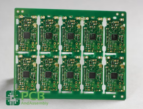
1. Surface Mount Devices (SMDs)
This is to be taken as being those electronic components directly located on the surface of a PCB. They are more miniaturized and compact, compared to the traditional components, and are thus best for modern electronic devices. Common components are resistors, capacitors, diodes, transistors, integrated circuits (ICs).
2. PCB Assembly Process
The process of assembly starts with a clean PCB, and solder paste is then applied to the PCB. Subsequent to SMD, there is an AVG action providing these components owing to an automated machine. Later, most of these components would be soldered using reflow soldering, referring to the board being heated to melt the solder and lock the components in place on the board.
3. Inspection and Testing
The PCB undergoes a number of tests following assembly to make sure everything went according to plan and that the parts’ dependability and quality are adequate. This is done automatically by AOI, X-ray, and sometimes functionality testing.
Advantages of Surface Mount Technology
SMT technology has many advantages over conventional conditions that have made it popular in the industry today and why most PCBs don’t get made without it anymore.
1. Compact Design
In the hypercritical area, surface-mount technology has the ability to make really compact and high-density circuit boards both because the given components are much smaller and there is not any through-hole drilling, which makes larger variations of the PCB obsolete; on the other hand, manufacturers can now produce the slimmest, most space-saving devices.
2. Higher Efficiency
SMT makes production faster. Thousands of components can be laid down in a minute very easily by automated machines on a PCB, making overall manufacturing efficiency excellent, especially when designing with mass production runs.
3. Reduced Costs
SMT assembly is cost-effective for several reasons. The use of smaller components and automated processes reduces labor costs. Additionally, the compact design of SMT-PCBs means that manufacturers can save on material costs, and the reduction in size can lower shipping and storage expenses.
SMT PCB Board Design Considerations
Designing a SMT PCB Board requires specific considerations to ensure successful manufacturing. Here are some critical design factors to keep in mind:
1. Component Placement
Proper placement of components is essential for efficient SMT assembly. Components should be arranged with an aim of minimizing the distance between them, permitting a smoother and faster manufacturing. Designers also have to think about the flow of heat through the components during the reflow process so they should be sure to place components in areas that can handle and confidently handle lots of heat without a PCB melt.
2. Trace Width and Spacing
The width of traces and between them have to be appropriately designed in order to prevent interferences of the electrical signal. Legal trace width assures the PCB can draw the required current without significant current/heating current flow. Right thickness of trace guarantees that the PCB is able to carry the intended current without massive temperature rise.
3. Soldering Considerations
It is a matter of great importance whatever kind of solder paste as it determines the quality of the solder joint. Also, the reflow temperature profile has to be tightly controlled to prevent deformation of the components or the PCB.
4. Thermal Management
Since SMT boards tend to be more compact, managing heat is critical. High-performance devices often generate significant heat, and the design must accommodate heat dissipation methods such as heat sinks or thermal vias to avoid overheating and component damage.
Future Trends in SMT and PCB Assembly
The future of products manufactured through surface mount PCB technology is quite enthralling to wait for. There is a continual pursuit of better SMT assembly technology that would make use of current techniques beyond what is used currently to provide even better layout capabilities.
1. Miniaturization of Components
The demand for smaller and more powerful consumer electronics equipment will constantly drive the trend for components to get smaller. Better manufacturing techniques would be needed to address the increasing complexity of SMT designs brought by the miniaturization trend.
2. Advanced Inspection Techniques
As PCBs become more complicated, sophisticated inspection methods are called for. Technologies such as X-ray inspection and 3D automatic optical inspection (AOI) are examples of new technologies currently being included in some processes to catch defects that were not visible earlier.
3. 3D Printing for PCB Manufacturing
The acceptance of 3D printing into PCB manufacturing is in its infancy. By some indication, designers can create more complex designs. As per one end of the spectrum, it provides for affordable rapid prototyping and highly customized PCB designs.
In Summary
Surface Mount Technology has transformed the way circuit boards are assembled, offering a host of advantages such as higher efficiency, smaller designs, and reduced costs. Since electronic devices will continue to develop, SMT will still be one of the key steps in the PCB assembly and manufacturing. Automation and new advancements in inspection technologies will allow manufacturing companies to continue to produce high-quality and fairly reliable PCBs needed in the fast-pace technological industries.

Get Quote Free