Three Common Printed Circuit Board Testing Methods
Get Your PCB Quote!

Table of Contents
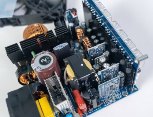
Any designer or builder who wants to achieve ultimate success must implement PCB testing methods. Circuit board testing can minimize major problems, identify minor errors, reduce costs, and save time. Let’s take a look at some of the most commonly used PCB testing methods.
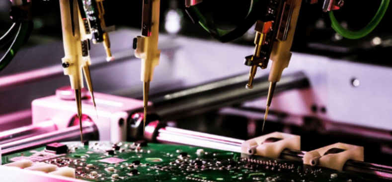
1. In-Circuit Test (ICT)
A probe connects the spring to each point of the circuit board. Each probe is given a 100-200g pressure by the spring to ensure good contact. The probes are placed in a “bed” of needles. Test points and signals are programmed by the software. Only probes that are required for testing the points to be tested are installed. The method of bed-of-needles allows for testing both sides at the same time. The test points should be on the soldering side of the board. The bed of needles tester is costly and hard to repair. The needle head can be configured to select different probes based on the application.
The basic universal grid processor is a board with pins that are spaced 100, 75, or 50 miles apart. The pins are probes that make mechanical connections directly with the electrical connectors on the board. A polyester film punched according to specifications is placed between the grid on the board and the pad to facilitate design-specific probes. The grid endpoints (defined as the coordinates x-y of the pads) are used to test continuity. Each net is independently tested to ensure continuity. The distance between the probes may limit the effectiveness.
1) Advantages:
√ Fast Test Speed
PCBA can be tested without turning on the power, reducing the time it takes to start the test and the risk of short circuits causing circuit boards to burn.
√ Excellent Testing Capabilities
It is controlled by a computer program that greatly reduces any risk of misjudging and missing tests, as well as the hassle of the production line.
√ Reduce Product Maintenance Cost
The maintenance of products can be done by operators, reducing costs. Computer programs can use ICT to identify which parts are faulty.
√ Improve Product Quality
ICT can measure the quality of the product by measuring all the lines on the circuit board as long as the test points are sufficient.
2) Disadvantages:
√ Long Preparation Time
It often takes several days or even weeks to make and debug the ICT needle bed fixture for an assembled printed circuit board.
√ High Production Cost
There is a production cost for the needle bed fixture every time. For some R&D companies and those with high market sensitivity, when they are eager to develop and launch new products, the ICT needle bed fixture cannot be debugged in time, or frequent product updates cause numerous ICT needle beds to be scrapped, resulting in huge cost waste.
√ Complicated Operation
The product line is too wide, resulting in the need for numerous ICT needle bed fixtures, making the operation steps complicated.
2. Using Observation Instruments
Because circuit boards have a complex and small structure, professional instruments are required to examine them. We use portable video microscopes to examine the structure of the circuit board. Video microscope cameras allow us to see the microscopic structures of circuit boards in a very intuitive way.
It is much easier to test and design circuit boards. PCB factories use video microscopes like the MSA200 or VT101 because they are more convenient to use than traditional microscopes.
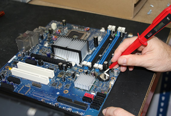
3. Double-Probe Flying Probe Test
Flying probe testers don’t rely on pin patterns that are mounted on fixtures or brackets. This system allows two or more heads to move freely within the x-y plane. CADI Gerber can control the test points directly. Dual probes are able to move up to 4 miles apart. The probes are not limited in their distance. The capacitance is measured by testers with two arms that can move in both directions. The second metal layer of the capacitor is a metal plate. The capacitance is larger at certain points if there is a break between the lines. The capacitance is reduced if there is a short between the lines.
The test speed is a key criterion in the selection of testers. A tester that uses a bed of nails can test thousands of points accurately at once, whereas a tester using a flying probe can only test a maximum of two or four points on the circuit board. A bed of nails tester can perform a one-sided test in 20-30 seconds, depending on how complex the board is, while a fly probe tester could take longer. Although high-volume printed board manufacturers find the moving probe test technology slow, it is still an excellent choice for circuit boards that are complex and have lower production volumes.
There are dedicated instruments for testing bare boards. Universal instruments are a more cost-efficient approach. These instruments may be initially more costly than dedicated instruments, but the initial cost is offset by a reduction in configuration costs. The standard grid size for universal grids is 2.5 mm. The test pads in this case should be larger than or equal to 1.3 mm. The test pads for a grid of 1 mm should be larger than 0.7 mm. The test needles will be small, brittle, and easy to damage if the grid is too small. It is therefore best to use grids larger than 2.5 mm. Combining a standard grid tester and a flying-probe tester with a universal tester will allow you to detect high-density boards in an accurate and cost-effective manner. A conductive rubber tester be used to detect deviations in the grid. The different heights between the hot air leveled pads and the test points will prevent the connection.
4. Summary
PCB inspection has many benefits. It ensures quality control for PCB boards. Inspections of PCB boards are a great tool to improve PCB production. You can fix a defect that tends to occur repeatedly at the level of the production process. PCB inspection is therefore important for the improvement of PCB production.
While it may be tempting to view it as a cost, the fact remains that without inspection, the cost of a product failure can be much higher. Inspecting the PCB can reveal any defects. In fact, inspecting the PCB after each stage helps to detect defects before moving on to the next stage. Inspection methods can help you ensure consistent quality in all aspects. Without proper inspection protocols, defective boards may make it to the market. When discovering product defects after shipment, recalls may become costly and reputation damage may ensue. PCB boards that contain errors can even put users in harm’s way with deadly results in vehicles or medical devices.
Multiple inspection techniques such as manual visual inspection, automated optic inspections, X-rays, functional PCB tests, etc. are used to ensure appropriate performance while maintaining an acceptable cycle time. Identifying the best technology to meet your project needs can go a long way toward ensuring PCB integrity.
At Pcbandassembly, we can meet all your PCB manufacturing needs. We are fully equipped to meet your PCB production requirements. Our expert team and the latest equipment we use ensure that our PCB boards are up to industry standards. It is our service philosophy of excellence that is the greatest guarantee of our success. If you need printed circuit board manufacturing or assembly, please feel free to contact us, we will be happy to provide you with our wholehearted service.

Get Quote Free