PCBA Circuit Board Fabrication: From Design to product
Get Your PCB Quote!

Table of Contents
As an ultramodern electronic manufacturing, Printed Circuit Board Assembly (PCBA) is crucial. From design to product requires a number of ways that each bear delicacy and specialised knowledge. Knowing how to perform the PCBA manufacturing process pivotal for contrivers, masterminds, and PCB Fabrication Manufacturer to insure top- quality and secure electronic products.
Designing the Circuit Board
The original step in PCBA product is the design phase which is where the masterminds design the circuit in relation to the purpose of the. This requires creating an illustration or schematic illustration, relating factors and constructing the PCB layout with technical software similar as Altium developer Eagle, and KiCad. The layout should maximise space, while icing high electrical performance, and minimum hindrance.
After the design has been perfected, the design is also subordinated to Design Rule Checking (DRC) to find any crimes, similar as duplicated traces, incorrect pad confines and distance problems. After this confirmation process is completed, the designs are exported in formats similar as Gerber as well as ODB for manufacturing.
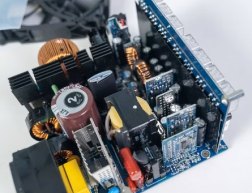
PCB Board Fabrication
Following the design phase, the PCB’s face is also constructed. This begins by opting an applicable substrate material; generally FR4 still high- frequency operations could use other accoutrements similar as Rogers. The fabrication process has several stages
1. The process of layering, lamination and multilayer PCBs need the lamination of numerous sub-caste of sheathe shells. Each sub-caste is strictly aligned and also clicked with pressure and heat.
2. Photoresist and Drawing: An image sub-caste is clicked to the PCB and UV light is employed to transfer the circuit’s pattern to the circuit board. The areas that are exposed are chemically etched in order to remove any board that isn’t needed, and leave only the traces that were designed.
3. Drilling and Plating Holes to factors are cut with perfection CNC machines. The holes are also carpeted with conductive material in order to produce electrical connections between the layers.
4. Solder Mask and Silkscreen operation: A guard of solder is put on to guard against accidental short circuits as well as the oxidation. The silkscreen sub-caste is applied to show element markers or ensigns as well as other markings.
Following these way the PCB is also subordinated to tests to check the electrical quality of the traces and connections.
Component Sourcing and Preparation
Before installation the electronic factors, they need to be linked and made. They’re named on the base of the Bill of Accoutrements (BOM) that specifies the PCB board manufacturer names, part figures as well as specifications. The quality of factors is pivotal to guaranteeing the quality of the final product.
Surface Mount Technology (SMT) factors are generally supplied in servers or rolls, and through- whole Technology (THT) corridor can be packed in bulk packaging. Every element has to be checked for quality and delicacy previous to installation.
PCB Assembly Process
When the PCB and all factors are set, the assembly process starts. This entails the positioning and the soldering of the factors onto the board by using automated as well as homemade styles.
1. SMT Operation with Solder Paste: The stencil printer and solder paste is used with PCB production. The paste is made up small patches suspended by flux which allows the factors to stick to the board previous.
2. Pick and Place Machine: Automated pick- and- place outfit positions SMT factors on the board with great perfection. These machines employ computer vision to insure precise placement, dramatically adding the speed of assembly.
3. Reflow Soldering: The board is passed through a flow furnace, in which controlled heating melts the solder paste and creates solid electrical connections between the rudiments and factors on the PCB.
4. Through- Whole Soldering: For factors that bear further solid mechanical bonds, like capacitors and connectors using through- whole soldering. This procedure can be fulfilled by hand or using surge soldering, in which PCBs are passed through a bow of solder that’s molten.
Examination and Testing
Once soldered, the completed PCB is subject to a rigorous examination and testing to insure its functionality and quality.
1. Automated optic examination (AOI): AOI systems make use of high- resolution cameras to identify problems with soldering, misaligned corridor as well as other problems. This non-contact approach provides rapid-fire and accurate blights discovery.
2. X-ray: X-ray examination for boards with solder joints hidden for illustration, Ball Grid Array (BGA) factors, Xray examination is employed to descry internal excrescencies similar as voids and the cold joints.
3. Functional Test: Functional test entails connecting power directly to a board and attesting the operation of the board in agreement with specifications for the design. This test assures that the PCB is operating as it should prior to it moving on to the coming stage of product.
Conformal Coating and Final Assembly
To increase the life, certain PCBAs are carpeted with conformal. The defensive sub-caste protects the board from dust, humidity or chemical pollutants. After the coating is applied the PCBA is part of the final quadrangle. Fresh factors like buttons, displays and connectors added when needed.
Quality Control and Compliance
Controlling quality is a pivotal element that’s essential to PCBA product. Manufacturers must cleave to norms like IPC- A610 for quality of assembly and IPC- 2221 to design PCBs. likewise, environmental and safety rules, similar as RoHS as well as ISO 9001, must be followed, to insure that final products is biddable with the conditions of transnational norms.
Spanning Up product
After the prototype has been validated and the prototype is supposed to be valid, product can commence. The process of spanning up requires careful planning in order to maximize effectiveness and drop charges. Factors like super eminent times, yields of product and logistics of force chain should be handled effectively. Ultramodern manufacturing styles like spare product along with Just- In- Time (JIT) control of force aid in reducing the time to produce large amounts.
PCBA circuit board manufacturing is a multi-step procedure which requires careful planning, perfection as well as quality assurance. Starting from the design stage through the final stage of product every step adds to the performance of the final product. As technology develops, advances like AI- driven design, automated examination, and high- tech accoutrements will continue to enhance the effectiveness and quality in PCBA manufacturing.

Get Quote Free