
Understanding Flying Probe Technology
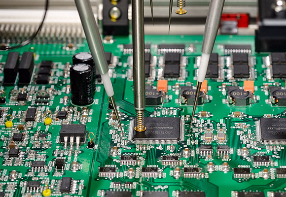
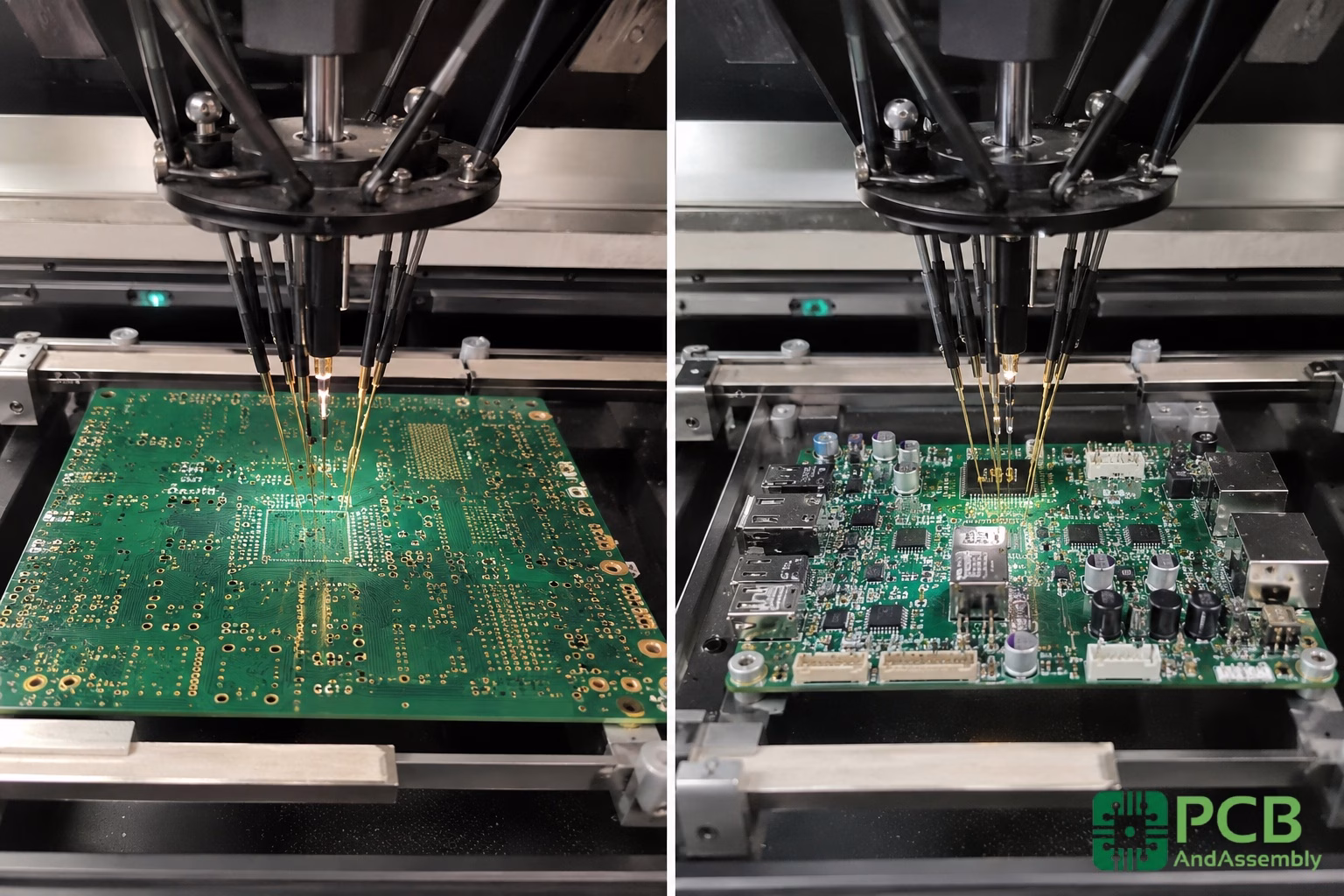
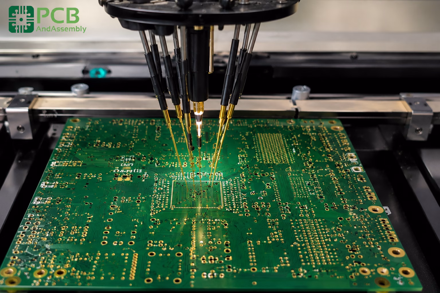
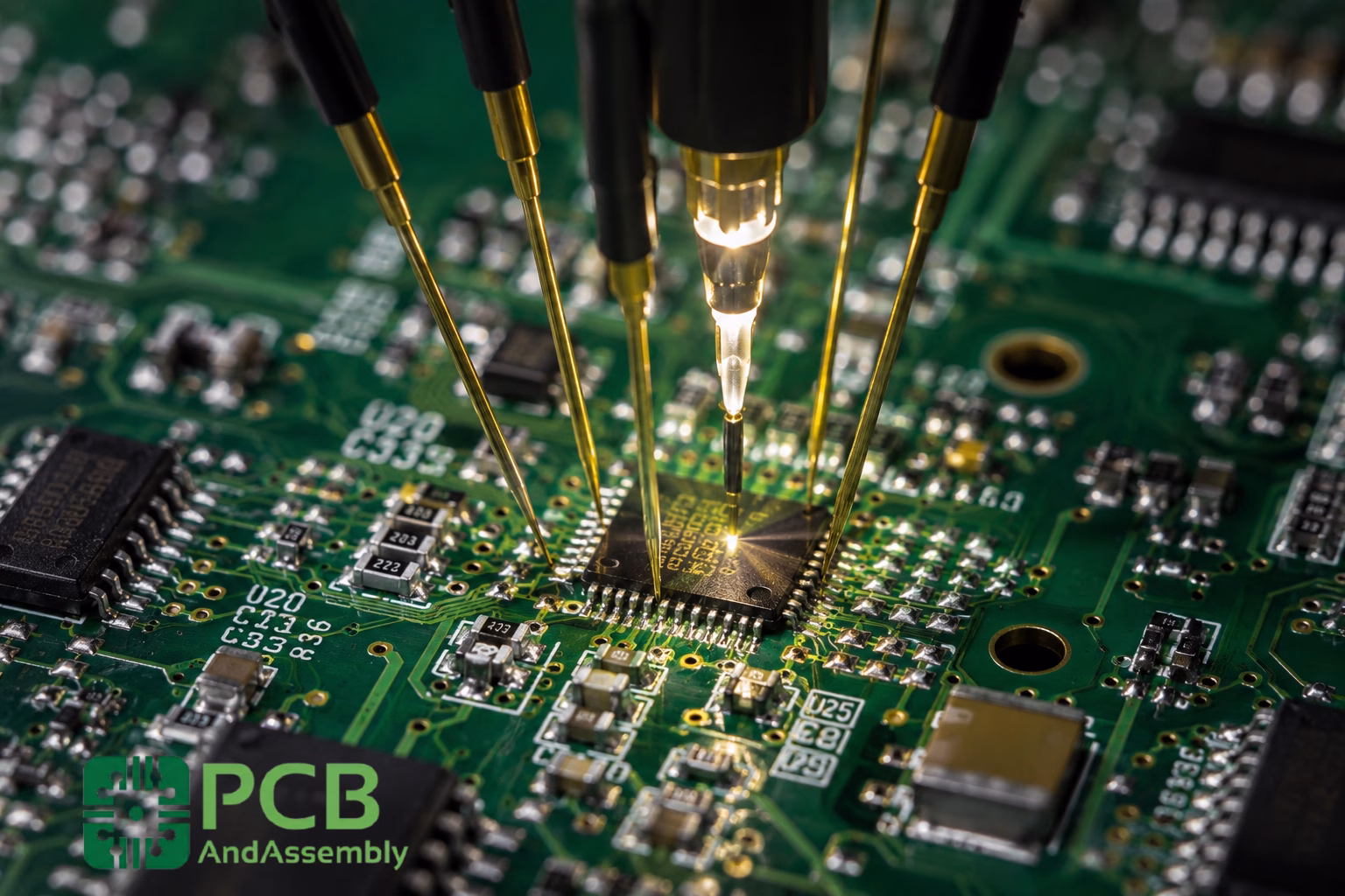
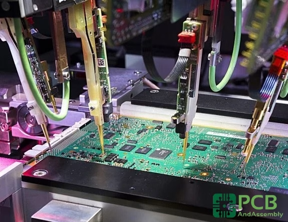
A flying probe tester is an automated electrical inspection system that positions movable probe heads — typically two to eight needles — to make precision contact with specific points on a printed circuit board. The probes travel freely across the board surface under the direction of high-accuracy servo motors and dedicated software, in contrast to conventional in-circuit test (ICT) fixtures that engage all test points simultaneously through a stationary bed-of-nails array.
The technology emerged in the late 1980s as a direct response to the cost and scheduling burden imposed by custom ICT fixtures. At the time, validating a new board design meant waiting weeks for a dedicated fixture to be designed and built — and paying a significant upfront fee before a single board was tested. Flying probe technology removed that barrier entirely, making electrical test accessible from the very first article.
How Flying Probe Testing Works
The underlying technology is sophisticated, but the operational workflow is straightforward:
Test Program Generation
Design data — typically in ODB++, IPC-2581, or Gerber format — is loaded into the flying probe software alongside the bill of materials. The system automatically computes probe paths, assigns measurement types to each net, and sequences the test routine for maximum efficiency.
Board Loading and Fixturing
Each PCB or PCBA is loaded onto the test platform and held in place using mechanical clamping, vacuum hold-down, or pneumatic fixturing. Optical fiducials on the board allow the system to calibrate probe positions to the actual board coordinates.
Probe Traversal and Contact
Motorized probe heads navigate in X, Y, and Z axes to contact each programmed test location in turn — landing on pads, vias, and component terminations per the test sequence. Contemporary systems routinely achieve positioning accuracy in the range of 10 to 15 micrometers, which is sufficient for fine-pitch and high-density designs.
Measurement and Evaluation
At each test point, the system applies a stimulus signal and records the electrical response. Measured values are compared against programmed pass/fail thresholds in real time, and any deviation is flagged immediately.
Results and Diagnostics
Upon completion, the system generates a detailed report covering pass/fail status for every net tested, with fault coordinates and measurement data for any detected failures.
What Flying Probe Testing Can Detect
Flying probe testing covers a broad spectrum of electrical defects. The table below summarizes the primary fault types and the measurement techniques used to identify them.
| Defect Category | Detection Method | Typical Target |
| Open circuits | Continuity measurement | Broken traces, cold solder joints |
| Short circuits | Isolation measurement | Solder bridges, copper debris |
| Resistance values | Ohmic measurement | Resistor value verification |
| Capacitance values | Capacitive measurement | Capacitor value verification |
| Inductance values | Inductive measurement | Inductor value verification |
| Diode orientation | Forward and reverse bias | Polarity verification |
| Component presence | Signature analysis | Missing component detection |
| Wrong component | Value comparison | Assembly substitution errors |
| Micro-shorts | High-voltage stress | Contamination, metallic whiskers |
In addition to these core measurements, advanced flying probe platforms extend their capabilities to include:
- Boundary scan testing through JTAG interface connections
- LED verification using integrated optical sensors to check color, polarity, and intensity
- In-circuit IC programming executed during the test sequence
- Thermal scanning to identify components operating outside normal temperature ranges
Flying Probe Testing for Bare PCBs vs. Assembled Boards
Flying probe testing is applied at two distinct points in the manufacturing process, each with a different focus and set of challenges.
Bare Board Testing
When applied to unpopulated substrates, flying probe testing concentrates entirely on the integrity of the copper network:
- Trace continuity across all copper layers
- Via connectivity, including through-holes, blind vias, and buried vias
- Net-to-net isolation across the entire board surface
- Impedance verification for controlled-impedance signal layers
- Detection of fabrication-introduced opens and shorts
At this stage, probes have unobstructed access to every pad and via on the board, enabling complete net coverage with minimal restriction.
PCBA Testing (Post-Assembly)
Testing an assembled board adds both capability and complexity. The scope expands to include:
- All bare board checks, now verifying that assembly has not introduced new electrical faults
- Solder joint integrity evaluation at accessible component terminations
- Component value and orientation verification against the bill of materials
- Basic functional verification where accessible test points allow it
The challenge at this stage is probe access. Ball grid arrays, chip-scale packages, and 0201 passives provide little or no opportunity for direct probing. Thorough design for testability (DFT) practices applied during layout are the most effective way to maintain coverage on populated boards.
| Aspect | Bare PCB Testing | PCBA Testing |
| Primary Focus | Board integrity and trace connectivity | Component and board verification combined |
| Timing | After fabrication, before assembly | After component placement and soldering |
| Net Coverage | Typically 95 to 100 percent | 70 to 95 percent depending on design |
| Test Speed | Generally faster | Slower due to added complexity |
| Probe Access | Unrestricted to all test points | Constrained by component placement |
| Defects Targeted | Fabrication defects only | Fabrication and assembly defects |
Flying Probe vs. In-Circuit Test: Selecting the Right Approach
This comparison arises in almost every test strategy discussion, and for good reason — both methods are valid, but they serve different operational conditions. Understanding the tradeoffs makes the decision straightforward.
Advantages of Flying Probe Testing
- No fixture investment: eliminates the $3,000 to $20,000-plus cost of a custom ICT fixture
- Rapid deployment: test programs are typically ready within hours to a few days
- Design agility: engineering change orders are accommodated through a software update, with no hardware rework
- Prototype-friendly: the economics favor flying probe for runs under 500 to 1,000 units
- Fine-pitch access: probes can target pads as small as 80 micrometers on capable systems
- Zero non-recurring engineering charges for tooling
Limitations of Flying Probe Testing
- Lower throughput: a typical board requires 5 to 15 minutes to test, compared to under one minute for ICT
- Sequential measurement: nets are tested one at a time rather than in parallel
- Restricted functional testing: complex powered-up functional sequences are difficult to execute
- BGA visibility: hidden solder joints under area-array packages cannot be directly probed
Cost and Lead Time Comparison
| Cost Factor | Flying Probe | In-Circuit Test (ICT) |
| Fixture Cost | None | $3,000 to $20,000 or more |
| Programming Cost | $500 to $2,000 | $1,000 to $3,000 |
| Setup Lead Time | Hours to a few days | Two to six weeks |
| Test Time per Board | 5 to 15 minutes | 30 to 60 seconds |
| Design Change Cost | Software update only | Fixture modification plus reprogramming |
| Economic Breakeven | Optimal under 500 to 1,000 units | Optimal above 1,000 to 5,000 units |
As a general guideline: if production volume falls below 500 boards, or if design revisions are anticipated, flying probe testing delivers better value in virtually every scenario. For stable, high-volume designs, ICT recovers its fixture investment quickly through superior throughput.
Design for Testability Guidelines
Layout decisions made early in the design process have a direct impact on what flying probe testing can achieve. The following guidelines, applied consistently, maximize test coverage and minimize per-board test time.
Test Point Dimensional Requirements
| Parameter | Minimum | Recommended |
| Test pad diameter | 6 mil (0.15 mm) | 20 mil (0.5 mm) |
| Via diameter | 8 mil (0.2 mm) | 10 to 12 mil (0.25 to 0.3 mm) |
| Test point pitch | 10 mil (0.25 mm) | 20 mil (0.5 mm) |
| Pad-to-component clearance | 8 mil (0.2 mm) | 12 mil (0.3 mm) |
Board Layout Considerations
Board Edge Clearance
Reserve a minimum of 6 mm (0.24 inches) along at least two opposing board edges to accommodate machine handling rails. This zone can be part of the board or allocated to panel waste material.
Fiducial Markers
Place at least three fiducials on the PCB itself (two positioned diagonally), not exclusively on panel waste. These reference points allow the probe system to compensate for any minor positioning offset or board stretch.
Via Accessibility
Leave vias without solder mask tenting wherever they will be used as probe targets. Tented vias can be contacted, but exposed copper provides more consistent and repeatable probe contact.
Component Height Restrictions
Limit component height on the probing side to 40 mm wherever possible. Tall components create exclusion zones that the probe head must navigate around, extending test time and potentially reducing coverage.
Test Point Clustering
Grouping test points geographically reduces probe travel distance. On densely populated boards, intelligent clustering can cut total test time by 20 to 30 percent without sacrificing coverage.
Surface-Mount Component Considerations
For fine-pitch SMD components, particularly in dense areas:
- Extend solder pads approximately 0.3 mm beyond component lead terminations to provide a dedicated landing zone
- Program probes to contact pad extensions rather than landing directly on component terminations
- For BGAs, QFNs, and other area-array devices, route critical nets to accessible vias or dedicated test pads elsewhere on the board
The Flying Probe Test Workflow
The following sequence describes the typical workflow from data preparation through production testing.
Step 1: Design Data Preparation
Assemble the following materials before engaging your test provider:
- CAD data: ODB++ is the preferred format for the cleanest data transfer; IPC-2581 and native EDA formats are also well supported. Gerber files can be used but require additional manual processing
- Bill of materials: a structured spreadsheet listing component values, tolerances, and reference designators
- Netlist: extracted from your EDA tool for net-to-component correlation
- Assembly drawings: to support component placement verification during programming
Step 2: Test Program Development
The test engineering team imports your design data and performs the following:
- Parses all net definitions and assigns test point locations
- Generates optimal probe path sequences (handled automatically by modern software)
- Configures measurement parameters appropriate for each component type and value
- Establishes pass/fail thresholds derived from BOM component tolerances
Program development for a board of moderate complexity typically requires four to eight hours of engineering time.
Step 3: Program Validation
Before committing to production testing, the program is validated on known-good boards:
- Baseline measurements are recorded across all test points
- Probe contact positions are adjusted to ensure reliable, repeatable landing
- Measurement parameters are fine-tuned to eliminate false failure conditions
- Critical net coverage is confirmed against the netlist
Step 4: Production Execution
During production testing, the workflow runs as follows:
- Boards are loaded manually or via automated conveyor feeding
- The test program executes the full measurement sequence
- Real-time pass/fail status is displayed and logged for each board
- Failing boards are marked and segregated for failure analysis
- Statistical process control data is accumulated for yield monitoring
Integrating Flying Probe Testing into a Broader Quality Program
Flying probe testing is most effective as one layer in a multi-method inspection strategy. No single technique catches every defect class; the goal is complementary coverage.
Recommended Inspection Sequence
- Bare PCB fabrication
- Flying probe test on bare board
- SMT assembly
- Solder paste inspection (SPI)
- Automated optical inspection (AOI)
- Flying probe test on assembled board, or ICT
- Functional test
- Final quality review
How Flying Probe Complements Other Methods
| Inspection Method | Primary Defect Coverage | Pairing with Flying Probe |
| AOI | Component placement errors, solder defects | Strong pairing — visual and electrical coverage are complementary |
| X-ray | Hidden solder joints under BGAs and QFNs | Strong pairing — covers the probe access gaps |
| SPI | Solder paste volume and registration | Upstream prevention reduces assembly defect rate |
| Functional test | System-level operation | Flying probe handles component-level verification upstream |
| Burn-in | Early-life failure mechanisms | Application-dependent; used for high-reliability programs |
AOI and flying probe testing used together typically achieve combined defect coverage exceeding 95 percent for most board designs.
Relevant Industry Standards
IPC Standards for PCB Electrical Testing
| Standard | Title | Relevance |
| IPC-9252A | Guidelines for PCB Electrical Testing | Defines test methods, isolation voltages, and continuity thresholds |
| IPC-6012 | Qualification for Rigid PCBs | Performance specifications including electrical test requirements |
| IPC-A-600 | Acceptability of Printed Boards | Visual inspection criteria for bare boards |
| IPC-A-610 | Acceptability of Electronic Assemblies | Inspection criteria for assembled boards |
| IPC-2221 | Generic Standard for PCB Design | Design rules including testability requirements |
IPC Class Test Requirements
| IPC Class | Target Application | Electrical Test Requirements |
| Class 1 | Consumer electronics | Basic continuity and isolation verification |
| Class 2 | Industrial and telecom equipment | 100 VDC isolation, 10-ohm continuity threshold |
| Class 3 | High-reliability, aerospace, medical | 250 VDC isolation, minimum 100 Mohm insulation resistance |
| Class 3/A | Military and avionics | 250 VDC isolation, 100 Mohm insulation, 10-ohm continuity |
Input File Formats
- ODB++: the preferred format for flying probe program generation — richest data content with fewest translation errors
- IPC-2581: a vendor-neutral alternative with strong EDA tool support
- Gerber with drill files: widely accepted but requires more manual setup during programming
Major Flying Probe Equipment Manufacturers
- SPEA (Italy) — precision systems with advanced optical alignment
- Seica (Italy) — Pilot series testers, including simultaneous double-sided configurations
- Takaya (Japan) — broad product range spanning prototype through production volumes
- Acculogic (Canada) — combined flying probe and ICT platform solutions
- ATG Luther and Maelzer (Germany) — specialists in bare board electrical test
When to Select Flying Probe Testing
The decision framework below reflects the scenarios where flying probe testing delivers the best outcome.
Conditions That Favor Flying Probe Testing
- Production volume falls below 500 to 1,000 units
- The project is in prototype, pilot, or new product introduction (NPI) phase
- Design revisions are expected or actively in progress
- Schedule pressure makes a multi-week fixture lead time unacceptable
- Fixture investment is difficult to justify at current volumes
- The board design is highly complex, dense, or unconventional
- Quick turnaround — days rather than weeks — is required
Conditions That Favor Alternative Methods
- Production volume exceeds 5,000 units with a stable, frozen design
- Per-board test time must stay under one to two minutes
- The test plan requires complex powered functional sequences
- Fixture investment is justified by long production horizon and volume certainty
Frequently Asked Questions
What files are needed to set up a flying probe test?
Three items cover most requirements: design data in ODB++ format (preferred), IPC-2581, or native EDA output; a bill of materials in spreadsheet format with component values, reference designators, and tolerances; and Gerber files with drill data if a native format is not available. ODB++ provides the most complete data transfer and results in the fastest program generation with the fewest programming questions.
How long does testing take per board?
Test duration scales with board complexity. Simple boards with a limited number of nets typically complete in three to five minutes. A moderately complex production board usually takes five to fifteen minutes. Dense multilayer boards with thousands of test nets can require twenty to thirty minutes per board. This is measurably slower than ICT, but the tradeoff is zero fixture cost and same-day test availability.
Can flying probe testing inspect BGA solder joints?
Not directly. The solder balls under a BGA are physically inaccessible to probes. However, flying probe testing can confirm net connectivity through vias or test pads that are electrically connected to BGA pins via the board routing. For direct visualization of BGA solder joint quality, X-ray inspection is the appropriate complementary method.
What is the smallest pad size a flying probe system can contact?
Most production flying probe systems can reliably contact pads at 6 mil (0.15 mm) or larger. Some advanced systems, including certain SPEA configurations, achieve contact on micro-pads down to 50 micrometers. The practical minimum depends on the specific tester and probe configuration — always confirm the capability with your test service provider against your actual design.
Is flying probe testing practical for high-volume production?
Generally not. For runs above 5,000 units on a stable design, ICT fixture costs amortize quickly and the throughput advantage becomes decisive. That said, some manufacturers continue using flying probe at higher volumes when design instability, BOM changes, or the cost of fixture maintenance outweighs the throughput benefit. It is a situation-specific calculation rather than a hard rule.
Flying Probe Equipment Configurations
Not all flying probe testers offer the same capabilities. Understanding the equipment options helps when evaluating test service providers or selecting capital equipment.
Single-Sided vs. Double-Sided Systems
Single-sided systems deploy probes on one board surface at a time. They are less expensive to acquire and operate, and they work well for boards where most test points are accessible from a single side. Testing both surfaces requires a board flip and a second test cycle, adding handling time and complexity.
Double-sided systems operate probes simultaneously on both the top and bottom surfaces. This configuration significantly reduces test time for boards with components or test points on both sides. Current-generation double-sided systems can accommodate component heights up to 40 mm on each side while probing the opposite surface.
Horizontal vs. Vertical Board Orientation
Horizontal systems hold the board flat during testing. This is the most common configuration and integrates cleanly with standard automated handling conveyors.
Vertical systems hold the board upright during testing. This layout conserves floor space and handles large, heavy boards more effectively. Vertical configurations are often selected for testing backplanes or large panel arrays.
Probe Count and Speed
| Probe Configuration | Typical Use Case | Relative Throughput |
| 4 probes, single-sided | Simple boards and prototypes | Lowest |
| 6 to 8 probes, double-sided | Standard PCBA production | Moderate |
| 12 to 16 probes | Complex boards and medium volume | High |
| 20 or more probes | High-complexity and higher volume | Highest |
Higher probe counts enable concurrent measurement across multiple net pairs, reducing overall test cycle time substantially on complex boards.
Common Challenges and Solutions
Even well-configured flying probe programs encounter recurring challenges. The following covers the most common issues and how experienced test engineers address them.
Probe Marks on Test Pads
Flying probes leave small contact impressions on the pads they land on. For boards where cosmetic appearance is a concern, this can be flagged as a defect. Modern systems use controlled contact force to minimize mark depth, and programming probes to land on non-critical pad areas or via annular rings rather than primary solder pads reduces visible impact. Some systems offer zero-force optical probe confirmation for sensitive surfaces.
Probe Access in High-Density Areas
Boards with tight component spacing leave limited room for probe approach paths. The most effective mitigation is planning probe accessibility during the layout phase — routing critical nets to dedicated test vias away from dense component clusters. When probe gaps are unavoidable, boundary scan or X-ray inspection can cover the inaccessible region.
False Failures from Flux Residue
Flux residue or other surface contamination on test pads causes intermittent contact resistance, producing false reject results. The preferred solution is specifying a no-clean flux formulation compatible with electrical probing. Where that is not possible, board cleaning prior to testing eliminates the problem. Flying probe systems with automated probe cleaning features wipe contact tips between landings to maintain consistent measurement quality.
Extended Test Time on Large Boards
Boards with thousands of nets and widely distributed test points can take 30 minutes or more per cycle. Modern path optimization algorithms address most of the efficiency gap automatically. For applications where throughput is genuinely critical, panel testing — running multiple smaller boards in a single fixture-free setup — can recover significant cycle time.
High-Frequency Circuit Characterization
Standard resistance and capacitance measurements do not fully characterize high-speed signal integrity on RF or high-frequency digital traces. Flying probe systems equipped with impedance measurement capability address this for controlled-impedance verification. For specialized RF characterization, dedicated impedance test equipment used in conjunction with flying probe testing provides the most complete picture.
Advanced Flying Probe Capabilities
Modern flying probe platforms go well beyond basic continuity and component verification. The following capabilities extend the technology into areas that were previously outside its scope.
Boundary Scan (JTAG) Integration
Flying probe systems with integrated JTAG support can execute boundary scan test patterns by contacting the JTAG interface pins on the board. The probes establish connections to TDI, TDO, TMS, TCK, and TRST, enabling the boundary scan engine to verify connections to otherwise inaccessible components including BGA-mounted ICs and complex digital devices. The combination of physical probing and boundary scan covers more of the board than either technique alone.
LED Function Verification
Boards populated with indicator LEDs can be verified using flying probe systems equipped with integrated optical sensors. The probe system energizes each LED circuit while the optical sensor confirms that the LED illuminates at the correct color and within an expected intensity range. This catches polarity reversals, incorrect current-limiting resistor values, and defective LED components in a single automated step.
High-Voltage Stress Testing
Standard isolation measurements use modest voltages that may not reveal marginal defects such as micro-shorts between closely spaced traces or contamination-induced leakage paths. High-voltage stress (HVS) testing applies elevated voltages — typically in the 250 V to 1,000 V range — to force latent defects to manifest before the board reaches the field. This capability is particularly relevant for:
- Automotive electronics exposed to voltage transients and thermal cycling
- Power supply boards with high-voltage traces running at near-clearance spacing
- Medical devices where long-term reliability is a regulatory requirement
- Aerospace and defense applications with IPC Class 3/A test requirements
Thermal Imaging
Advanced flying probe platforms with integrated thermal sensors can detect abnormal component temperatures during powered testing. Elevated temperature at a specific component can indicate a shorted junction, an incorrect component value drawing excess current, or a solder joint with elevated contact resistance. Thermal scanning adds a functional dimension to what is otherwise a purely electrical measurement.
Industry Applications
Flying probe testing serves a range of industries with distinct quality requirements.
Automotive Electronics
Automotive systems must operate reliably across wide temperature and vibration ranges throughout a vehicle’s service life. Flying probe testing provides the electrical verification step before boards are integrated into vehicle systems where rework is costly or impossible. Most Tier 1 automotive suppliers combine flying probe testing with 100 percent AOI and periodic X-ray sampling to satisfy IATF 16949 quality management requirements.
Medical Devices
Medical electronics are subject to regulatory traceability requirements that demand complete documentation of every inspection step. Flying probe testing generates detailed, board-level test records that support FDA design verification submissions and quality system audits. The absence of custom tooling also suits the iterative design cycles common in medical device development, where design modifications may occur across multiple prototype iterations.
Aerospace and Defense
Military and aerospace programs typically specify IPC Class 3 or Class 3/A test parameters, requiring higher isolation voltages and tighter continuity thresholds than commercial electronics. Flying probe testing meets these requirements while accommodating the low-volume, high-mix production environment typical of defense manufacturing, where the number of unique board types often makes dedicated ICT fixtures economically impractical.
Consumer Electronics
Consumer product volumes typically favor ICT for production testing, but flying probe testing plays an important role during prototype development and new product introduction. Rapid program turnaround allows consumer electronics teams to validate multiple design iterations in a compressed timeframe, supporting aggressive launch schedules.
Industrial and Telecommunications Equipment
Industrial controls and telecom infrastructure frequently involve high-layer-count boards with mixed technologies and demanding performance specifications. The ability to handle diverse board types without dedicated tooling makes flying probe testing well suited to the varied product mix these industries require.
Business Case: Flying Probe vs. ICT Cost Analysis
Quantifying the financial tradeoff helps make the case for the appropriate test approach when volume and design stability are known.
Prototype Run Cost Comparison (50 Boards)
| Cost Element | ICT Approach | Flying Probe Approach |
| Fixture cost | $8,000 | $0 |
| Test programming | $2,000 | $1,000 |
| Lead time to first test | 4 weeks | 3 days |
| Per-board test cost ($10/board) | $500 | $500 |
| Total | $10,500 | $1,500 |
The economic advantage narrows as volume increases. The crossover point — where ICT fixture cost is offset by lower per-board test time costs — typically falls between 500 and 2,000 units, depending on board complexity, test time, and the fully loaded cost of operator time.
Indirect Benefits Beyond Direct Cost
The financial case for flying probe testing extends beyond fixture avoidance:
- Time-to-market: test availability measured in days rather than weeks accelerates the product launch timeline
- Design freedom: engineering changes are implemented as a software update with no tooling cost or lead time
- Inventory reduction: no obsolete fixture assets when designs are revised or discontinued
- Diagnostics quality: detailed coordinate-level fault data reduces failure analysis time
- Operational flexibility: one set of equipment handles the full range of board designs in the product portfolio
Summary
Flying probe testing has established itself as a core tool in PCB and PCBA quality assurance, with particular strength in the prototype and new product introduction phase where design flexibility and rapid deployment matter more than raw throughput speed.
The technology continues to advance. Current systems offer faster probe velocities, sub-10-micrometer positioning accuracy, and an expanding set of integrated capabilities including boundary scan, optical verification, and high-voltage stress testing. For engineering and manufacturing teams working with complex boards, variable production volumes, or evolving designs, flying probe testing provides a level of coverage, cost efficiency, and operational agility that fixture-based approaches cannot replicate.
The key is proper integration into a comprehensive test strategy. Flying probe testing combined with AOI, X-ray inspection where warranted, and a functional test step at the end of the line delivers defect coverage that protects both product quality and program schedule. Whether the goal is validating a first prototype, qualifying a production process, or maintaining quality across a diverse product mix, flying probe testing offers a proven and practical solution.