Preventing Cold Solder Joints in PCB Assembly
A seemingly minor flaw, a cold solder joint can lead to intermittent connections, increased resistance, and ultimately, device failure, making its prevention a top priority in PCB assembly.
Get Your PCB Quote!
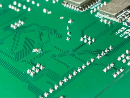
Table of Contents
- 1Que sont les joints de soudure froids ?
- 2L’impact critique des soudures froides sur la fiabilité des circuits imprimés
- 3Causes profondes des soudures froides
- 4Méthodes de détection efficaces des joints de soudure froide
- 5. Joints de soudure à froid complets Stratégies de prévention dans l'assemblage de circuits imprimés
- 6. Cet les sites anciens Splus Joints QFPs
- 7. Résumé
- Points clés à retenir
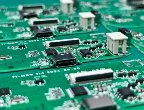
In the intricate world of Printed Circuit Board Assembly(PCBA), the quality of every solder joint is paramount to the long-term reliability and performance of electronic devices. One of the most common and critical defects that can compromise this quality is the “cold solder joint”. A seemingly minor flaw, a cold solder joint can lead to intermittent connections, increased resistance, and ultimately, device failure, making its prevention a top priority in manufacturing.
This guide delves deep into the phenomenon of cold solder joints, exploring their characteristics, the severe impact they have on PCB reliability, and the underlying causes. More importantly, we provide a comprehensive set of strategies for detection and, crucially, prevention, ensuring robust and dependable PCB assembly. Understanding and implementing these measures is essential for engineers, technicians, and anyone involved in the PCB assembly process to maintain high standards of quality and avoid costly rework or product recalls.
1. What Are Cold Solder Joints?
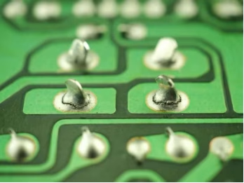
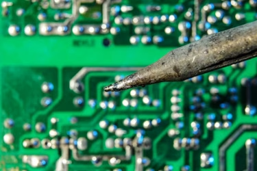
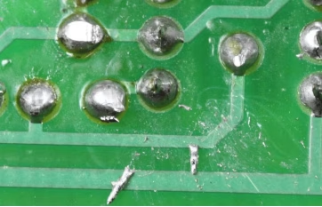
A cold solder joint occurs when the solder does not properly melt and fuse with the component lead and the PCB pad. Instead of forming a smooth, shiny, and concave connection, a cold solder joint appears dull, gritty, lumpy, or even cracked. It signifies a poor metallurgical bond, resulting in a weak electrical and mechanical connection.
Visually, a good solder joint is characterized by a shiny, smooth, and uniform surface, with a concave fillet that “wets” both the component lead and the PCB pad. In contrast, a cold solder joint exhibits:
- Dull and Grey Appearance:Lacks the metallic luster of a properly flowed joint.
- Rough or Granular Texture:The surface may feel coarse rather than smooth.
- Lumpy or Blob-like Shape:Solder forms an irregular mound instead of a smooth fillet.
- Poor Wetting:Solder does not spread evenly across the pad and lead; it might bead up.
- Pinholes or Cracks:Small voids or visible cracks can indicate an incomplete bond.
These visual cues are critical for initial detection and highlight the inadequate adhesion between the solder and the metal surfaces, which is the root of its unreliability.
2. The Critical Impact of Cold Solder Joints on PCB Reliability
The presence of cold solder joints can have far-reaching and severe consequences for the functionality and longevity of electronic products. While some might consider them minor aesthetic flaws, their impact is profoundly functional:
- Intermittent Connections:The most common issue, leading to erratic circuit behavior, signal dropouts, or devices that only work intermittently. This can be incredibly difficult to diagnose.
- Increased Electrical Resistance:A poor metallurgical bond means higher resistance at the joint. This can lead to signal degradation, power loss, and localized heating, potentially damaging other components over time.
- Component Failure:The increased resistance and heat can stress components, leading to premature failure. This is especially critical for sensitive components.
- Short Circuits:In some cases, poor wetting or excessive solder due to a cold joint can bridge adjacent pads, causing unintended short circuits.
- Mechanical Weakness:Cold solder joints offer little mechanical integrity, making them susceptible to failure under vibration, thermal expansion/contraction, or physical stress.
- Reduced Product Lifespan:Devices containing cold solder joints are prone to early failure, leading to customer dissatisfaction, warranty claims, and damage to brand reputation.
For critical applications like medical devices, automotive electronics, or aerospace systems, the implications of such failures are not just financial but can also pose safety risks. Therefore, diligent prevention and detection are non-negotiable.
3. Root Causes of Cold Solder Joints
Understanding the causes of cold solder joints is the first step toward effective prevention. These defects often stem from a combination of factors related to temperature, material quality, technique, and environment.
3.1 Insufficient Heat
This is arguably the most common cause. If the soldering iron temperature is too low, or if the dwell time is too short, the solder will not reach its melting point and flow properly. Similarly, components with high thermal mass may draw heat away too quickly, preventing the joint from reaching the optimal temperature for proper wetting.
3.2 Contamination and Oxidation
Dirty PCB pads, component leads, or oxidized solder can all prevent proper wetting. Oxides on metal surfaces act as a barrier, preventing the solder from forming a strong metallurgical bond. Dust, grease, or flux residues can also interfere.
3.3 Component Movement During Cooling
If a component is moved or vibrated while the solder is still solidifying(between its liquid and solid states), the fragile bond can be fractured, leading to a dull, granular appearance and a mechanically weak joint. This is often referred to as a “dist urbed joint”.
3.4 Incorrect Solder Alloy or Old Solder
Using the wrong type of solder for the application, or solder that has degraded over time(e.g., old solder wire with evaporated flux), can lead to poor flow characteristics and cold joints. Solder paste also has a limited shelf life.
3.5 Insufficient or Depleted Flux
Flux plays a critical role in cleaning metal surfaces and aiding solder flow by reducing surface tension. If there’s too little flux, or if it depletes before the solder properly melts and wets, oxidation can persist, leading to a cold joint.
3.6 Poor Soldering Technique
In manual soldering, inconsistent operator technique, such as applying solder before the joint is adequately heated, uneven heat distribution, or insufficient solder application, can directly result in cold solder joints.
3.7 Excessive Solder
While seemingly counterintuitive, applying too much solder can sometimes mask a cold joint by creating a large blob that hides poor wetting underneath. It can also make it harder for heat to properly penetrate to the joint interface.
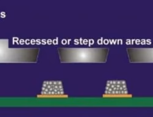
3.8 Inadequate Pad Design or Thermal Relief
For pads connected to large ground planes or traces, proper thermal relief is crucial. Without it, the pad acts as a heatsink, drawing away too much heat and making it difficult to achieve proper solder temperature.
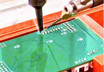
4. Effective Detection Methods of Cold Solder Joints
Detecting cold solder joints requires a combination of visual inspection and advanced testing techniques. Early detection is crucial to prevent further processing of faulty boards and reduce rework costs.
4.1 Visual Inspection
This is the primary and most accessible method. Trained operators use magnification(microscopes or magnifiers) to look for the characteristic signs of cold solder joints:
- Dull, rough, or gritty appearance.
- Lumpy, irregular, or spherical solder blobs.
- Poor wetting, where solder doesn’t flow smoothly onto the pad and lead.
- Cracks or voids within the solder joint.
Consistency in lighting and operator training are vital for effective visual inspection.
4.2 Automated Optical Inspection(AOI)
For high-volume production, AOI systems are indispensable. These machines use cameras to capture images of solder joints and compare them against a predefined set of parameters for good joints. AOI can quickly identify deviations in shape, volume, and reflectivity that indicate cold solder joints.
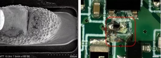
4.3 X-ray Inspection(AXI)
For components where solder joints are hidden from view(e.g., Ball Grid Arrays-BGAs, or Quad Flat No-leads-QFNs), X-ray inspection is essential. AXI can reveal internal structural defects, voids, or inadequate solder fill, which are indicative of cold solder joints or other issues that cannot be seen externally.
4.4 Electrical Testing
While not directly identifying a cold joint’ s appearance, electrical tests can detect its functional consequences:
- In-Circuit Test(ICT):Measures resistance, capacitance, and other electrical parameters of individual components and connections. A cold joint will likely present as an open circuit, high resistance, or incorrect component value.
- Functional Test:Simulates the operational environment of the final product to verify that the PCB functions as intended. Intermittent failures during functional testing often point to cold solder joints.
5. Comprehensive Cold Solder Joints Prevention Strategies in PCB Assembly
Preventing cold solder joints is far more cost-effective than detecting and reworking them. A proactive approach involves meticulous attention to detail at every stage of the PCB assembly process.
5.1 Optimal Temperature Control
- Proper Iron Temperature:For manual soldering, ensure the iron is set to the correct temperature for the solder alloy being used and adjust for the thermal mass of the component. Typically, 350-400°C(662-752°F) for lead-free solder and 30 0-350°C(572-662°F) for leaded solder.
- Adequate Dwell Time:Ensure enough contact time for the joint to reach soldering temperature.
- Preheating:For wave soldering or components with high thermal mass, preheating the PCB helps reduce thermal shock and ensures uniform temperature across the board, allowing solder to flow more efficiently.
- Reflow Oven Profiles:Calibrate reflow ovens precisely according to solder paste specifications, ensuring the correct ramp-up, soak, reflow, and cooling zones.
5.2 Maintain Impeccable Cleanliness
- Component Leads & PCB Pads:Always ensure component leads and PCB pads are clean and free from oxidation, dust, and grease. Use clean gloves when handling components and boards.
- Solder Materials:Use fresh, high-quality solder and solder paste. Store them according to manufacturer recommendations to prevent oxidation and flux degradation.
- Equipment Maintenance:Regularly clean soldering iron tips, nozzles, and reflow oven interiors to prevent contamination and ensure consistent performance.
5.3 Ensure Component Stability
- Secure Components:Prevent any movement of components during the soldering and cooling phases. Use jigs, fixtures, or tape to hold components firmly in place until the solder has fully solidified.
- Minimize Vibration:Ensure the work area is stable and free from vibrations that could disturb newly formed solder joints.
5.4 Correct Solder and Flux Selection
- Matching Solder Alloy:Always use the correct solder alloy for the application(e.g., leaded vs. lead-free) and ensure it’s compatible with the component finishes.
- Appropriate Flux:Select the right type and amount of flux. Flux cleans the surface and aids solder flow. Ensure it’s active enough but doesn’t leave harmful residues.
- Fresh Materials:Solder paste and flux have limited shelf lives. Adhere to expiration dates and proper storage guidelines.
5.5 Skilled Operators and Consistent Technique
- Comprehensive Training:Thoroughly train operators in proper soldering techniques, including iron handling, solder application, and visual inspection of completed joints.
- Standard Operating Procedures(SOPs):Implement clear SOPs for all soldering processes to ensure consistency and repeatability across all operators and shifts.
- RegularSkill Audits: Periodically assess operator skills and provide refresher training as needed.
5.6 Design for Manufacturability(DFM)
- Pad Design:Ensure adequate pad size and shape for proper solder wetting.
- Thermal Relief:Implement thermal relief designs for pads connected to large copper planes to prevent excessive heat sinking, allowing the joint to reach temperature more easily.
5.7 Regular Equipment Calibration and Maintenance
- Soldering Stations:Calibrate soldering irons and stations regularly to ensure accurate temperature readings. Replace worn-out tips promptly .
- Reflow Ovens/Wave Solder Machines:Perform routine maintenance and calibration to ensure temperature profiles and mechanical movements are precise and consistent.
Need PCB Manufacturing or Assembly?
Get a free quote within 24 hours. We specialize in prototype-to-production PCB/PCBA for hardware teams worldwide.
6. Cold Solder Joints FAQs
Question1: Can cold solder joints be repaired?
Yes, cold solder joints can often be repaired by reheating the joint with fresh flux and sometimes a small amount of new solder. The goal is to allow the solder to fully reflow and form a proper metallurgical bond. However, prevention is always better as repeated rework can stress components and pads.
Question2: What is the difference between a cold solder joint and a dry joint?
These terms are often used interchangeably to describe a poor solder connection due to insufficient heat or poor wetting. Both result in a dull, gritty appearance and a weak bond. A “dry joint” specifically implies a lack of proper fusion due to inadequate wetting, often caused by impurities or insufficient flux, leading to a poor electrical connection.
Question3: Do lead-free solders make cold solder joints more likely?
Lead-free solders typically have higher melting points and a narrower plastic range compared to leaded solders. This means they require more precise temperature control and can be more susceptible to cold joints if proper thermal profiles and techniques are not meticulously followed.
Question4: How can I identify a cold solder joint without special equipment?
For through-hole components, you can often visually inspect the joint under good lighting, perhaps with a magnifying glass. Look for a dull, rough, lumpy, or grainy appearance instead of a smooth, shiny, concave fillet. Sometimes, wiggling the component can reveal an intermittent connection if the joint is extremely poor.
7. Summary
Cold solder joints represent a significant threat to the reliability and performance of PCB assemblies, leading to issues ranging from intermittent connections and increased resistance to complete device failure. These defects arise primarily from insufficient heat, contamination, component movement during cooling, and improper soldering techniques or materials. Visually, they are characterized by a dull, rough, or lumpy appearance, lacking the smooth, shiny fillet of a healthy joint.
Effective detection relies on keen visual inspection, supplemented by advanced methods like Automated Optical Inspection(AOI) for surface-mount components and X-ray Inspection(AXI) for hidden joints. However, the most effective strategy is comprehensive prevention. This involves strict adherence to optimal temperature control during soldering, maintaining impeccable cleanliness of all materials and equipment, ensuring component stability during the cooling phase, selecting appropriate solder and flux, training skilled operators with consistent techniques, and incorporating Design for Manufacturability(DFM) principles. By prioritizing these preventive measures, manufacturers can drastically reduce the occurrence of cold solder joints, leading to more robust, reliable, and longer-lasting electronic products.
Key Takeaways
- Cold solder joints are weak, dull, and rough connections due to inadequate solder flow and bonding.
- They cause critical reliability issues like intermittent connections, increased resistance, and component failure.
- Primary causes include insufficient heat, contamination, component movement, and incorrect materials/techniques.
- Detection relies on visual inspection, AOI, AXI, and electrical testing(ICT, functional).
- Prevention requires precise temperature control, material cleanliness, component stability, correct solder/flux, skilled operators, and DFM.
- Proactive prevention is crucial for high-quality, dependable PCB assembly and product longevity.

Get Quote Free