How Do You Avoid PCBA Welding Problems?
Get Your PCB Quote!

Table of Contents
Although there is no reliable way to avoid welding problems completely, we can still take a series of good practices during PCB design and PCBA welding to reduce the possibility of encountering welding problems.
1. Pay Attention to Welding Mask Design
The welding mask layer is usually green and covers the thin polymer coating on the surface of the PCB. It is designed to protect the copper layer from environmental pollutants. In addition to preventing oxidation, the welding mask layer also has the function of putting a stop to welding bridging, because welding has difficulty adhering to the coating. Therefore, it is recommended to design the welding mask layer between the pads to form a welding mask dam. This is particularly beneficial for components with small pad gaps such as IC and BGA.
2. Reasonable Placement of Fiducial Marks
Fiducial marks are circular welding mask openings with a circular exposed copper layer in the center, which should be set on the board during the PCB design stage. For components that require special handling, there are panel fiducial marks and individual component fiducial marks. The placement machine uses these marks as reference points on the PCB to align the SMD components on the board during the SMT patch process. If applied correctly, fiducial marks can improve the placement accuracy of components. However, if the fiducial marks are not designed properly (e.g., improperly positioned or with insufficient fiducials), this can lead to inaccurate positioning, increasing the risk of welding problems.
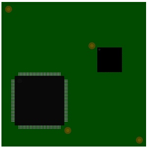
Positioning of the fiducial mark on the printed circuit board
3. Maintaining the Cleanliness and Tinning of the Welding Iron Tip
The quality of hand welding will be directly affected if the welding iron tip is not properly maintained. Any contaminants or oxidation on the tip will reduce its thermal conductivity and thus affect the quality of the welding joint. Therefore, it is important to pay attention to welding techniques. Before welding, always wipe the tip with a cleaning pad to ensure it is clean. If the tip is severely oxidized, it can be repaired with a special activator. Dip the tip into the activator and gently move it to allow the abrasive to work until the tip surface is restored to a shiny state.
After completing the above steps, the tip should also be tinned. Tinning is to cover the tip with a layer of welding to prevent oxidation and improve its thermal efficiency. It is recommended to clean the tip after welding two or three joints and again after each welding job. This practice will help to extend the life of the welding iron and improve the quality of the welding joint.
4.Perfection Through Practice
welding is a skill that will be improved with practice. Before you tackle those precious and fragile projects, you can practice on scrap circuit boards or welding practice boards. Try different welding techniques, find the method that best suits your operating habits, determine the best time to combine welding and welding iron tips, and continue to learn and correct mistakes in practice.
To improve the convenience of welding, pen-like micro-welding irons have been launched on the market. This type of welding iron integrates temperature display and control circuits into the handle, making the welding process easier and smoother.
5. Cooperate with a Professional Printed Circuit Board Assembly Factory
If you think that manual welding and self-sourcing components are too cumbersome, or consider that using micro components is beyond your operating range, it will be a wise decision to choose to cooperate with an experienced professional PCBA processing factory. You can avoid many problems during the PCB assembly process in this way.

Get Quote Free