How To Assemble Own PCB Solder Mask?
Get Your PCB Quote!

Table of Contents
The solder mask is a special surface layer on a Printed Circuit Board. It is usually made of organic resin and its main purpose is to enhance the performance and protect the PCB. Solder masks usually sit on top of weld surfaces and perform a number of functions, including preventing short-circuits, increasing reliability and insulation.
1. What Is a Solder Mask?
Solder masks are thin polymeric layers that are applied on the surface of PCB boards. The main component is either solder paste or actual solder. Solder masks are used to prevent solder from seeping through onto copper circuits during soldering, so that only pads remain uncovered by this layer of solder mask. Solder pastes are typically made up of ingredients like flux, solder and other materials. They’re intended to be soldered to electronic components in the PCB assembly.
Solder masks can be applied at the top and bottom PCB. The resin is used as the main component in the solder mask. It is resistant to moisture, temperature and is also non-conductive. The solder mask used on most PCB boards was initially green, hence the term “green oil”. Soldering masks come in a variety of colors, including black, green, yellow, and white. There are several factors that determine the color of a solder mask.
The solder mask layer is a part of the printed circuit board. It is also described in electronic design automation as a Gerber, just like other layers, such as screen and copper. These layers are commonly known as tStop/bStop (EAGLE), LSMVS/LSMRS (WEdirekt), or GTS/GBS (Gerber, etc.)
Solder bridges are the green oils that run between two pads, or IC pins. They’re called solder masks bridges because they have a narrow requirement. It is best to cancel the solder bridge if the distance between pins is not sufficient to meet the factory’s process.
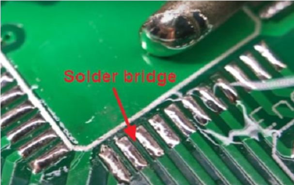
The ink color, and the thickness of copper are related to the process manufacturing capability of the solder bridge. Solder mask bridges with green oil are easier to control and can be kept at a minimum. As the thickness of copper increases, the solder bridge will get larger. Thin copper has a smaller solder bridge and is easier to work with than thick copper.
Minimum Solder Mask Bridge Width:
Green oil 0.075 mm, other variegated colors 0.125 mm (red, yellow, blue, white, matte green, black, matte black, purple and so on)
2. What Is the Function of the Solder Mask?
Solder masks are mainly made of liquid UV light imaging dyes. There are many colors available, including green, red and blue. Solder mask layers on PCB boards perform a variety of functions.
Prevent Short Circuits
Solder masks are important for preventing short circuits on PCB boards. Solder paste spillage and poor soldering can occur when soldering PCB components without protection from the solder mask. The result will be a short circuit between the components. Solder masks can isolate the soldering area to prevent short circuits.
Improve Weld Quality
The solder mask can also improve precision and quality by controlling the size and shape of the welding area. The solder mask reduces the area of the weld, increases the accuracy, prevents uneven or excessive flow of solder, and makes sure that the quality meets standard requirements.
Strengthen Mechanical Components
A solder mask increases the mechanical strength of a PCB and makes it more durable. The solder mask acts as a sort of overlay to fix components and connect lines, preventing damage to the PCB from the external environment. During PCB assembly, and during transportation, the solder mask can protect the Printed circuit Board’s surface from mechanical vibrations and collisions.
Improved Moisture Resistance
Solder masks have good sealing properties and can prevent moisture, dust, and other impurities entering the PCB. This protects the components of the circuit board against environmental factors. It is crucial for electronic devices which require high reliability, long-term durability and are used in moist environments.
Inspection and Maintenance Convenient
Solder masks make the PCB surface more flat and convenient for inspections and maintenance. Solder masks are useful for reducing repair costs, accelerating workflows and preventing damage to other components when troubleshooting and replacing parts.
Eco-Friendly and Aesthetically
Solder masks can help reduce pollution emissions. This is very environmentally friendly. Furthermore, solder masks provide another layer of protection to PCB colors and appearance, making the PCB look more professional.
Solder layers not only strengthen and secure boards, but they can also serve to shield components from external influences and facilitate inspection and repair processes. Solder masks improve the reliability and performance of the board and also simplify the manufacturing process and reduce maintenance costs. They can also improve production efficiency.
3. Types of Solder Masks
PCB boards come in different solder mask types. The board is thermoset after the pattern is determined. Solder masks come in three main categories:
Epoxy Liquid
There are different types of solder masks depending on their application. The cheapest solder mask available is an epoxy liquid screen-printed on a PCB.
LPSM (Liquid Light Imaging Solder Mask)
LPSM is screen-printed on a PCB or sprayed onto it. The pattern can then be exposed and developed so that an opening can be made in the pattern to allow the part to be soldered directly to the copper pad.
DFSM (Dry Film Light Imaging Solder Mask)
DFSM is vacuum laminated on a PCB and then exposed to light.
4. How to Assemble the PCB Solder Mask?
The PCB drawing has a soldering mask layer, divided into two layers: top and bottom. This is easily understood from its literal meaning, which means to prevent soldering. How does this layer actually solder mask?
First, let’s look at the pads:
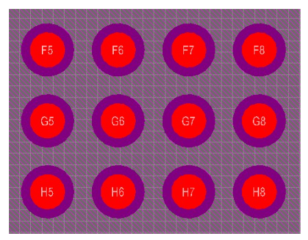
This is a pad in a BGA package. On the bottom layer you can see a pattern similar to this. The PCB is removed and only the red portion in the middle can be soldered. All other parts, such as the purple area, cannot be soldered. This is the solder mask. We received the PCB and found it to be green, red, or any other color. The color of the layer was the green oil that we read about on the internet.
How does this solder mask layer correspond to the green oil? Solder masks are represented on PCB as negative sheets. The sheet with the soldering mask can be exposed. If you don’t use a soldering mask, the area will turn green, and you won’t be able to weld. If you think about it, the negative is that the board should be covered with green oil. However, if there’s a solder mask somewhere, then the oil has to be removed. This is subtraction. Solder masks should be used wherever there are pads. Otherwise, the board is wasted.
Let’s now look at how to make a solder mask!
1) Process Flow
Solder mask→ filming, filming, positioning holes→ cleaning of printed circuit boards→ preparation of inks→ double-sided printing→ pre-baking→ exposure→ development → thermosetting
Step 1, Clean the Board: Clean the surface of the board. Remove all dirt and grime, and dry the surfaces.
Step 2, Ink Application: In the second step, you will need to place the cardboard in the vertical crater. By considering factors like robustness, we can determine the thickness. The width of the solder mask can vary when it is located in different areas on the board.
Step 3, Pre-hardening: Pre-hardening is different from complete hardening. Stabilize your coating. You can remove unnecessary layers during the development phase.
Step 4, Imaging and Hardening: Place a transparent sheet of film on the plate. Combining it with a schematic drawing, and then exposing it to ultraviolet radiation. A transparent film was used to partially cover the solder mask. The film is covered with a circuit drawing and adhered to the pre-hardening. Assures correct alignment during hardening. The foil can be prevented from being exposed by aligning it properly. This vulnerability can affect functionality or cause a short-circuit.
Step 5, Development: At this level, the PCB is placed in a developer for cleaning any unwanted solder mask. This ensures that the copper foil required is visible.
Step 6, Final Hardening and Cleaning: The final step is to perform the final hardening. I did this to mount the solder mask on the PCB surface. Before further processing, you need to clean the plates. It can be done in the form or assembly, surface finish.
2) Analysis of Key Processes
Pre-Baking
Pre-drying has the purpose of evaporating the solvent in the ink so that the solder mask film is in a non-sticky state. The temperature of the pre-baking and duration will differ depending on what type of ink you are using. Pre-baking temperatures that are too high, or drying times that are too long will result in poor development and reduced resolution. If the temperature or time of pre-baking is too low or too short, then the film will adhere to the film and the sodium carbonate will erode the solder-mask film, which will cause the surface to lose luster and the solder-mask film to fall off.
Exposure
The key to any process is exposure. The solder mask at the edge reacts to light and forms a residual layer when exposed too much. This is due to light scattering. The test can reflect this situation: when the exposure time is longer, the line width measured is negative; for short exposure times the line width measured is positive. The “light energy integrated” can be used in the actual process to determine the best exposure time.
Adjustment of Ink Viscosity
The ratio of hardener and main agent, as well as the amount of diluting agent added, are the two most important factors that determine the viscosity. Ink characteristics can be affected if the hardener amount is not sufficient. The viscosity of the ink changes after mixing hardener at room temperature.
Within 30 min: If the main ink agent, hardener, and fluidity are not fully integrated, then the screen will block during printing.
30 min~10h: The main ink and hardener are fully integrated, and the fluidity has been adjusted.
After 10 hours: Inks are more fluid and difficult to print because of this active reaction. The ink luster will also improve if you wait longer after mixing the hardener. After mixing the hardener, you can start printing after 30 minutes to get a glossy ink and good printability.
The ink will become harder and less heat-resistant if you add too much thinner. The viscosity of liquid photosensitive Solder Mask Ink must be adjusted. If it is too thick, screen printing will be difficult. Stencil easily sticks to the net. The ink viscosity and volatile solvent content are too high, making pre-curing difficult.
A rotary picometer is used to measure the viscosity. The optimal viscosity value is adjusted in production according to the different inks, solvents, and other factors.
5. Summary
The solder film on a printed circuit board serves as a permanent protective coating that not only performs the functions of protection, solder mask and insulation resistance, but has also a significant impact on the board’s appearance. Solder mask was first used to create screen graphics and then UV curing inks. Due to screen deformation and incorrect positioning, excess solder film is left on the pad after each printing. Removing this takes a long period of time and requires a large amount of manpower. The liquid photosensitive solder ink can be used without screen graphics and with contact exposure. This process is high-alignment accurate, has good adhesion to solder mask and resistance, and produces high output. It has gradually replaced light setting inks.
Solder masks can be used both for manual and automated assembly. The solder mask plays a vital role in the PCB manufacturing process. This is crucial for the best performance and connection.

Get Quote Free