
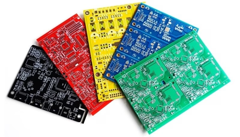
If you have spent years tracking down intermittent signal integrity failures on high-density assemblies, you know that chasing defects post-reflow is an expensive , frustrating game. I have spent over a decade watching engineers tweak reflow profiles or blame component finishes, only to trace up to 70% of their defects back to the stencil printer. Implementing 3D Solder Paste Inspection (SPI) was the single biggest turning point for our surface mount technology (SMT) first-pass yield rates.
The stencil printing step seems deceptively straightforward: a squeegee blade pushes solder paste through laser-cut stencil apertures onto copper pads. However, once you scale down to 0201, 01005, or even 03 015 component packages, the physical margin for error shrinks to near zero. A minor variation in paste volume, a microscopic clog in a stencil aperture, or a slight misalignment can manifest as a tombstone, a head-in-pillow ( HiP) joint, or a bridge. 3D SPI acts as the primary quality gate in the SMT line, catching these volumetric printing errors before components are placed and the board enters the reflow oven.
What Is 3D Solder Paste Inspection?
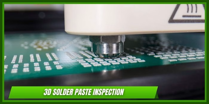
3D Solder Paste Inspection is an automated optical measurement system positioned between the stencil printer and pick-and-place machine in an SMT assembly line. Its job is to verify that every solder paste deposit meets specifications for volume, height, area, and position before components are placed.
Unlike manual visual inspection or basic 2D camera systems, 3D SPI creates a complete topographical map of each paste deposit. It uses structured light projection or laser triangulation to measure the actual three-dimensional shape of the solder paste, not just its footprint.
Why Solder Paste is a Three-Dimensional Engineering Problem
Early SMT lines relied on manual visual inspection or 2D automated optical inspection (AOI) systems. These legacy systems analyzed solder paste deposits based purely on a two-dimensional overhead footprint . They evaluated the area coverage and horizontal alignment (X and Y coordinates) of the paste deposit, but they were entirely blind to the Z -axis.
Solder paste is inherently a three-dimensional fluid-structure. Its behavior is governed by rheology, viscosity, and surface tension. Two printed deposits can appear identical from an overhead 2D camera —both covering 100% of the pad area and aligned perfectly with the pad borders. However, if the first deposit has a height of 120 µm and the second has a height of only 50 µm due to paste shearing or stencil clogging, their volumes differ by more than 50%. The 2D system will pass both boards. The 50 µm deposit, however, will likely result in an open circuit or a structurally weak, lean fillet after reflow. Conversely , a deposit with excessive height will lead to solder balls or bridging to adjacent pads.
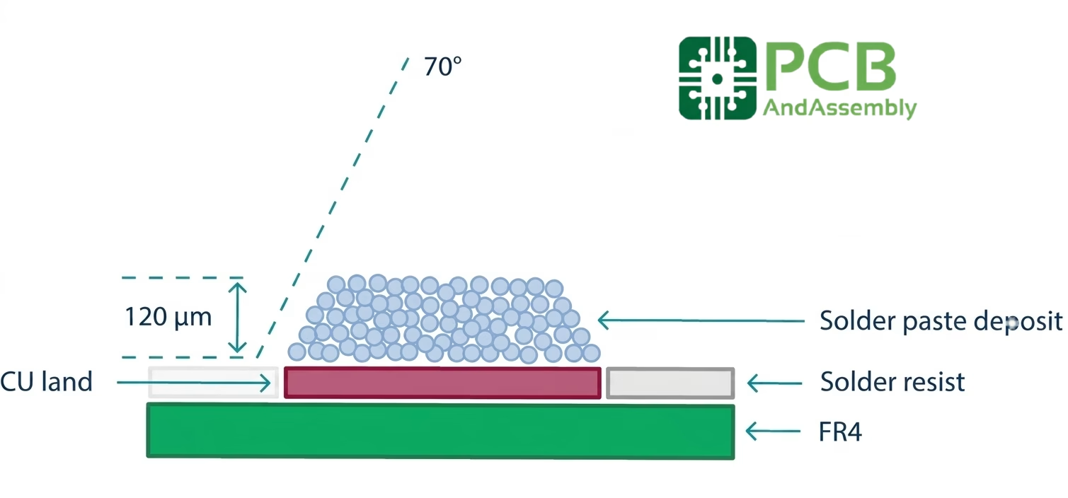
As component pitches shrink, the ratio of the stencil aperture area to the aperture wall area—known as the Aspect Ratio and Area Ratio—becomes a limiting factor in paste release. When the Area Ratio drops below 0.66, the cohesive forces binding the paste to the aperture walls frequently overcome the adhesive forces holding the paste to the copper pad, leading to incomplete paste transfer. 3D SPI is the only method capable of verifying paste transfer efficiency by measuring the exact volumetric topography of each deposit.
| Parameter | 2D SPI Capability | 3D SPI (Laser Triangulation) | 3D SPI (Fringe Projection) | Impact on SMT Yield |
| Area Measurement | Yes ( Grayscale contrast) | Yes (High accuracy) | Yes (Ultra-high accuracy) | Detects pad coverage and initial smearing. |
| X/Y Alignment | Yes (Centroid analysis) | Yes (Laser line scanning) | Yes (Structured light) | Prevents bridging and offset-induced tombstoning. |
| Height Profiling | No | Yes (Triangulation geometry) | Yes (Phase-shifted point cloud) | Identifies high/low deposits that cause opens or HiP. |
| Volume Calculation | Estimated (Highly inaccurate) | Calculated (± 5% accuracy) | Calculated (±2% accuracy) | The primary metric determining post-reflow joint integrity. |
| Inspection Speed | Fast (2D capture) | Moderate (Mechanical scanning) | High (Multi-frequency projection) | Maintains line beat rate even on high-density boards. |
Laser Triangulation vs. Fringe Projection: Choosing Your Measurement Method
Modern 3D SPI systems rely on optical met rology to reconstruct the three-dimensional surface profile of the solder paste. Two primary technologies dominate the industry: Laser Triangulation and Structured Light Fringe Projection (often utilizing Moiré interferometry).
Laser Triangulation
Laser triangulation systems project a highly focused laser line or spot onto the PCB surface at a known angle. A high-speed digital camera, positioned at a complementary angle, captures the reflected laser profile. When the laser crosses a raised object—like a deposit of solder paste—the line shifts laterally from the perspective of the camera. By calculating the physical displacement of this laser line using trigonometric equations, the system maps the exact height profile of the paste. The sensor head or the PCB is moved mechanically to scan the entire board surface, line by line, to build a complete topographical dataset.
Fringe Projection (Phase-Shift Moiré Technology)
Structured light systems project a series of Ronchi grating patterns (fringe patterns consisting of alternating light and dark stripes) onto the PCB. As these stripes fall across the three-dimensional contours of the solder paste, the straight lines distort. By projecting multiple phase-shifted patterns (typically shifting the phase by 90-degree increments), a sensor captures the deformed fringes. Proprietary vision algorithms analyze the phase modulation at every pixel to generate a high-density 3D point cloud of the board’s surface. This method captures large areas simultaneously, offering rapid inspection cycle times.
I strongly recommend choosing phase-shift structured light projection over laser triangulation for high-mix, high-density SMT lines. In my experience , laser-based systems suffer from micro-shading on fine-pitch 0.4 mm BGA pads, which leads to false-positive failures and slows down cycle times. Additionally, fringe projection systems do not require continuous mechanical scanning of the optical head in the Z-axis, reducing mechanical wear and maintaining much higher repeatability over a 10-year equipment lifespan.
Setting Solder Paste Inspection Limits Under IPC-7527
The global standard governing solder paste printing and inspection parameters is IPC-7527 (Requirements for Solder Paste Printing Processes). This document provides the guidelines for establishing process windows, measurement tolerances, and quality classes. To build an effective inspection program, you cannot simply use the default machine limits. You must tailor your SPI thresholds to your specific stencil thickness, aperture designs, and component pitches .
The four primary metrics measured by 3D SPI systems are Height, Area, Volume, and Position Offset. Setting limits that are too tight leads to high false-call rates, which forces operators to constantly press the “bypass ” button, defeating the purpose of automated inspection. Setting limits too loose allows defective prints to pass through, resulting in costly post-reflow rework.
| Metric | Typical IPC-75 27 Target | Practical Limits
(Fine Pitch / 0201) |
Failure Mode if Out of Range |
| Height | 100% of stencil thickness | 80% to 140% of nominal thickness | & lt;80%: Insufficient solder, weak fillets. >140%: Bridging, solder ball ing. |
| Area | 100% of aperture CAD area | 85% to 115% of target area | <85%: Poor wetting , potential open joints. >115%: Solder paste smear, bridging. |
| Volume | 100% calculated volume (Area x Height) | 70% to 130% (High density) 80% to 120% (Standard ) |
<70%: Joint starving, head-in-pillow. >130%: S older shorts, excessive fillets. |
| Position Offset | 0. 00 mm (Perfect alignment) | < 25% of pad width (Class 1, 2, 3) | >25% alignment deviation: Tombstoning, component shifting. |
I have seen boards come back with massive head-in-pillow (HiP) defects on BGAs because the SPI limits were set too wide—specifically, allowing paste height to drop to 70 % of stencil thickness. For any component with a pitch of 0.5 mm or less, I enforce a strict lower limit of 80% on height and 75% on volume. This ensures there is sufficient flux and alloy mass to break through the surface oxide layer during the reflow phase, preventing the component balls from sitting on top of a partially melted paste deposit without coalescing.
How Shadowing and Board Warp Distort Measurement Data
Optical metrology is only as accurate as the light it can capture. Two physical phenomena constantly threaten the integrity of 3D SPI data: optical shadowing and PCB warpage.
The Shadowing Problem
In high-density boards, tall pre-existing components, dense connector housings, or adjacent high-volume solder paste deposits can block the projected light from reaching the valleys of smaller, neighboring pads. Single-sided light projection systems suffer from this limitation; they cannot inspect what they cannot illuminate. This shadow zone prevents the system from capturing the complete fringe pattern, leading to inaccurate volume calculations.
To overcome this, premium SPI systems utilize dual-projection or quad-projection optical configurations. By projecting structured light from opposite directions (e.g., East/West or North/South/East/West) and combining the resulting images through advanced vision algorithms, the system eliminates shadow zones. Any area shadowed from the left light source is fully illuminated by the right light source, guaranteeing a complete 3D topographical reconstruction of the entire deposit.
The Board Warp Problem
Printed circuit boards are rarely perfectly flat. During handling, clamping, and transport , organic laminates like FR-4 undergo physical bowing, twisting, and shrinkage. In a standard SMT line, a PCB can easily warp by up to 1.0 mm or more across its length.
If an SPI system uses an absolute Z-axis reference plane based on the machine’s mechanical conveyor rails, a warped PCB will distort all height measurements. For example, if a portion of the board is bowed upward by 80 µm, a perfectly printed 120 µm solder paste deposit will register as 200 µm high. The system will trigger a false-fail flag for excessive paste. Conversely, downward bow leads to false-fails for insufficient height.
To prevent this, advanced SPI systems employ Active Warp Compensation. Before calculating paste height, the system sweeps the board surface to detect local PCB surface heights. Using infrared sensors or rapid optical triangulation, the system calculates a dynamic 3D surface model of the substrate. It then establishes a “local zero” reference plane for every single pad on the board, subtracting the local PCB warp from the absolute measurement. This ensures that the measured height of the solder paste is calculated relative to the copper pad surface , not the machine gantry, preserving measurement repeatability even on thin, highly warped substrates.
Connecting SPI to Stencil Printers and Pick-and-Place Systems
In a modern smart factory environment, 3D SPI does not operate as an isolated island of data. It serves as the analytical brain of the printing section of the line, communicating upstream to the stencil printer and downstream to the pick-and-place machine via standardized protocols like SMEMA, IPC-CFX, or proprietary Machine-to-Machine (M2M) software interfaces.
Upstream Feedback Loop to the Stencil Printer
When the SPI system detects a repeating trend of position misalignment ( e.g., paste deposits consistently shifting 30 µm to the left), it transmits offset correction data back to the stencil printer. The printer automatically adjusts its internal board alignment cameras to compensate for the drift on subsequent prints before the error exceeds the acceptable IPC tolerance limits.
Furthermore, SPI systems monitor paste buildup on the stencil. If the system detects a decline in paste volume or an increase in irregular shapes over a series of boards, it recognizes that the stencil apertures are becoming clogged. The SPI machine automatically sends a command to the stencil printer to initiate an under-stencil cleaning cycle (using wet, vacuum , or dry cycles). This predictive maintenance approach drastically reduces the frequency of manual interventions and prevents defect escapes.
Downstream Feed-Forward Loop to Pick-and-Place Machines
If a board exhibits minor, acceptable alignment offsets in its solder paste deposits, the SPI system can forward these exact coordinate deviations to the downstream pick-and-place machine . Rather than placing components at the theoretical CAD coordinates, the pick-and-place system dynamically shifts the component leads to match the actual center of the printed solder paste. This prevents component shifting during reflow, as the surface tension of the molten solder will pull the component into alignment rather than causing a tombstone.
Additionally, if a multi-panel PCB (matrix panel) contains a sub-board that has failed inspection due to catastrophic paste bridging or insufficient volume, the SPI system flags that specific board’s serial number. The downstream pick-and-place machine receives this data and performs an “NG Board Skip,” bypassing the bad panel to avoid wasting expensive active IC components on a substrate that is destined for the wash station.
Calculating the ROI of 3D SPI
Purchasing a 3D SPI machine is a significant capital expenditure, typically ranging from $60,000 to $120,0 00 depending on resolution, speed, and dual-projection capabilities. For procurement managers, proving the return on investment (ROI) is essential. Fortunately, the math supporting SPI implementation is compelling because of the Rule of Tens in electronics manufacturing: the cost of repairing a defect increases tenfold at each successive stage of production.
| Stage of Defect Detection | Cost per Defect | Required Action | Detection Tool |
| Post-Stencil Printing (SPI) | $0.50 | Wipe paste off board, clean, and reprint. No components wasted. | 3D SPI System |
| Post-Reflow / Pre-Test (AOI) | $5 0.00 | De-solder component, clean pads, hand-solder new component. Risk of board damage. | 3D AOI System |
| Functional Test (F CT) / ICT | $150.00 | Isolate defect, diagnose circuitry , manual rework, re-test board. | In-Circuit / Functional Tester |
| In the Field (End Customer) | $500.00+ | Warranty replacement, shipping costs, field service labor, reputational damage. | Customer Failure Report |
To illustrate a real-world scenario, let’s look at a mid-sized contract manufacturer producing 500 boards per day. Prior to installing 3D SPI, their post-reflow defect rate was 3%, resulting in 15 defective boards per day. Finding and reworking these defects at the post-reflow AOI stage cost approximately $50 per board, totaling $750 per day in rework labor, component loss, and scrap. After implementing a dual-projection 3D SPI system with an automated closed-loop feedback system, the post-reflow defect rate dropped to 0.5% (only 2.5 boards per day). The remaining 12.5 defects were intercepted immediately after the stencil printer. Wiping and reprinting these boards cost only $0.50 per board.
The daily cost of defects plummeted from $750 to $131.25, yielding a daily savings of $618.75. Based on a standard 250-day working year, this translates to $154,687 in annual savings. In this scenario, the 3D SPI machine pays for itself in less than eight months, while simultaneously increasing overall factory capacity by reducing the bottleneck at the manual rework stations.
Common Solder Paste Defects Detected by 3D SPI
Understanding the specific defect types that 3D SPI intercepts—and their root causes—is critical for closing the loop between inspection data and process improvement. Below are the primary failure modes encountered in SMT printing, along with typical corrective actions.
| Defect Type | 3D SPI Detection Method | Typical Root Cause |
| Insufficient paste volume | Low volume / low height flag | Clogged aperture, insufficient squeegee pressure, paste viscosity drift |
| Excess paste / bridging | Adjacent deposits connected in topography map | Over-pressure, excessive paste roll, poor snap-off speed |
| Position offset / misalignment | Centroid deviation beyond tolerance threshold | Printer alignment drift, stencil stretch, PCB fiducial error |
| Missing paste | No deposit detected on target pad | Fully blocked aperture, dry paste, PCB surface contamination |
| Smearing / paste spread | Area exceeds pad boundary in point cloud | Poor snap-off, stencil underside contamination, low paste viscosity |
Offset defects deserve particular attention on fine-pitch assemblies. A 50 µm position error that is barely noticeable on a 1206 pad represents roughly 25% of a 0201 pad width—enough to generate consistent tombstoning when combined with normal pick-and-place tolerance variation. This compounding effect is invisible to post-reflow AOI unless the process engineer traces the failure back to the SPI dataset. Establishing a systematic correlation practice between SPI data and downstream defect findings is the fastest path to process-level root-cause analysis.
3D SPI Equipment Selection Criteria
Not all 3D SPI systems deliver equal performance. When evaluating equipment for a new or upgraded SMT line, the following specifications separate capable systems from those that will generate excessive false calls or miss critical escapes.
| Specification | Minimum Acceptable | High-End Systems |
| Z-axis resolution | 1.0 µm | 0.5 µm |
| Z-axis accuracy | ±3 µm | ±1 µm |
| XY resolution | 15 µm | 10 µm |
| Measurement repeatability (GR&R) | <10% | <5% |
| Inspection speed | 50 cm²/s | >100 cm²/s |
| Minimum pad size | 0.15×0.15 mm | 0.08×0.08 mm |
Measurement repeatability—expressed as Gauge Repeatability and Reproducibility (GR&R)—is arguably the most important specification when comparing systems. GR&R quantifies how much of the total observed variation in measurement results comes from the instrument itself versus the actual process being measured. An SPI system with a GR&R above 15% will generate unacceptable noise: real process drifts become indistinguishable from measurement scatter, false calls increase, and operators begin bypassing the system. For high-density boards with tight paste volume tolerances, a GR&R below 5% should be treated as a non-negotiable requirement.
Software capability deserves equal weight alongside hardware specifications. Essential software features include Gerber and ODB++ import for automatic inspection program generation, statistical process control (SPC) with real-time trend visualization, closed-loop interfaces to both the upstream printer and downstream placement machine, and per-component tolerance adjustment. Systems that require manual pad-by-pad programming are unsuitable for high-mix environments where new board designs are introduced frequently.
Frequently Asked Questions
Q: Can we use a 2D AOI system positioned after the printer as a low-cost alternative to a dedicated 3D SPI?
A: No. A 2D system cannot measure paste height or volume. It is highly prone to false positives and, more critically, false negatives. While a 2D system can catch gross alignment errors or massive bridges, it will miss insufficient volume defects on fine-pitch components (like 0201s or 0.4mm pitch BGAs), leading to high escape rates of open solder joints that are only detected post-reflow.
Q: How long does it take to program a 3D SPI system for a new PCB design?
A: With modern SPI software, programming is highly automated. By importing the stencil Gerber file (usually in RS-274X or ODB++ format) and the ODB ++ board CAD file, the system automatically identifies pad locations and aperture sizes. Programming a standard, moderately complex board typically takes less than 15 minutes, making it highly suitable for high-mix, low-volume production environments.
Q: Does 3D SPI slow down the SMT line cycle time?
A: Modern high-speed fringe projection SPI systems can inspect up to 85 cm² to 100 cm² of board surface per second. For the vast majority of SMT lines, the inspection cycle time of the SPI is significantly faster than either the stencil printing cycle (typically 20 to 45 seconds) or the pick-and -place cycle. Consequently, the SPI system does not act as the line bottleneck.
Q: Can 3D SPI inspect alternative bonding materials like conductive glue or sinter paste?
A: Yes. Leading 3D SPI systems are equipped with multi-color lighting and adjustable optical parameters that allow them to accurately inspect and measure the volume of gray conductive glues, reflective silver sinter pastes, and flux-only deposits, expanding their utility beyond standard SAC305 solder paste.
Summary and Final Judgment
At the end of the day, buying a 3D SPI system is not about buying a fancy inspection camera; it is about establishing a robust insurance policy for your assembly yields. If you are building IPC Class 3 hardware or placing anything smaller than 0402s, skipping 3D SPI is no longer a viable way to save capital. The physical limits of solder paste transfer dictate that volumetric variation will occur; trying to manage an SMT line without measuring that variation is like trying to drive a car with a blacked-out windshield.
By investing in a dual-projection system with active warp compensation and integrating it into a closed-loop feedback configuration with your stencil printer, you move your quality control model from ” defect detection” to “defect prevention.” The initial capital investment is quickly offset by the reduction in rework labor, component scrap, and field failures. For any high-yield electronics manufacturing facility, 3D SPI is an essential tool.
Future Trends in 3D Solder Paste Inspection Technology
The 3D SPI market continues to advance rapidly. Several development directions will shape how these systems are deployed and utilized over the next several years.
AI and machine learning integration is the most significant near-term shift. Rather than relying on fixed volumetric thresholds, next-generation SPI systems learn from accumulated historical inspection data to distinguish genuine defects from borderline-acceptable process variation. This substantially reduces false-call rates without sacrificing escape protection, allowing process engineers to tighten real defect detection while reducing operator intervention.
Enhanced Industry 4.0 connectivity is becoming a baseline expectation rather than a premium option. Standards like IPC-CFX (Connected Factory Exchange) and HERMES are enabling seamless, vendor-agnostic data sharing between SPI systems, stencil printers, pick-and-place machines, and enterprise MES platforms. This real-time data fabric makes it possible to perform cross-line yield optimization and centralized monitoring from a single dashboard.
Expanded inspection scope is another trend worth tracking. Leading SPI vendors are extending the same optical measurement platforms to inspect adhesive dispensing, conformal coating thickness, and selective solder deposits. For contract manufacturers running diverse product mixes, this reduces the total number of dedicated inspection systems required on the floor.
Recommended Resources
For engineers looking to go deeper on solder paste inspection standards, process control methods, and equipment evaluation, the following references provide authoritative guidance.
IPC Standards (available at ipc.org):
IPC-7527 (Requirements for Solder Paste Printing), IPC-7525 (Stencil Design Guidelines), and IPC-A-610 (Acceptability of Electronic Assemblies) together form the foundational framework for establishing and auditing a compliant paste inspection program.
Industry Publications:
SMT Magazine (iconnect007.com) and Circuits Assembly Magazine (circuitsassembly.com) regularly publish application case studies and equipment reviews covering 3D SPI deployments. Application notes from major vendors including Koh Young, CyberOptics, Viscom, and Mycronic provide detailed measurement methodology documentation and benchmark data useful for equipment comparison.
Training and Certification:
IPC online training courses and SMTA (Surface Mount Technology Association) webinars offer structured learning paths for process engineers implementing or optimizing SPI systems. Equipment manufacturer training programs are the fastest route to system-specific programming and calibration proficiency.
