
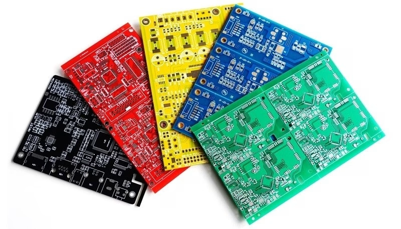
A few years ago, we audited a production line for high-density industrial controllers, which achieved a first-pass yield of 98% at the In-Circuit Test (ICT) stage.On paper, the project was a success. However, three months into field deployment, the return rate for “no-power” and “inter mittent signal” failures spiked. When we cross-sectioned the boards, we found the culprit: micro-cracks in the solder joints under a 0.8mm pitch BGA. The cause wasn’t the reflow oven or the component quality—it was the ICT fixture itself. The mechanical pressure required to make contact with 1,200 probes was flexing the 1.6mm FR-4 just enough to fatigue the corner joints of the most rigid components.
This is the reality of In-Circuit Testing. While it is often marketed as the “gold standard” for high-volume manufacturing (HVM) because of its speed and diagnostic precision, it is also a high-impact mechanical event . If you treat ICT as a purely electrical gate, you are missing the risks it introduces to your assembly’s long-term reliability. In this guide, we will walk through the technical specifications of ICT, the critical Design for Test (DFT) requirements , and the specific failure modes we have encountered in over 15 years of high-volume PCBA production.
What Is In-Circuit Testing?
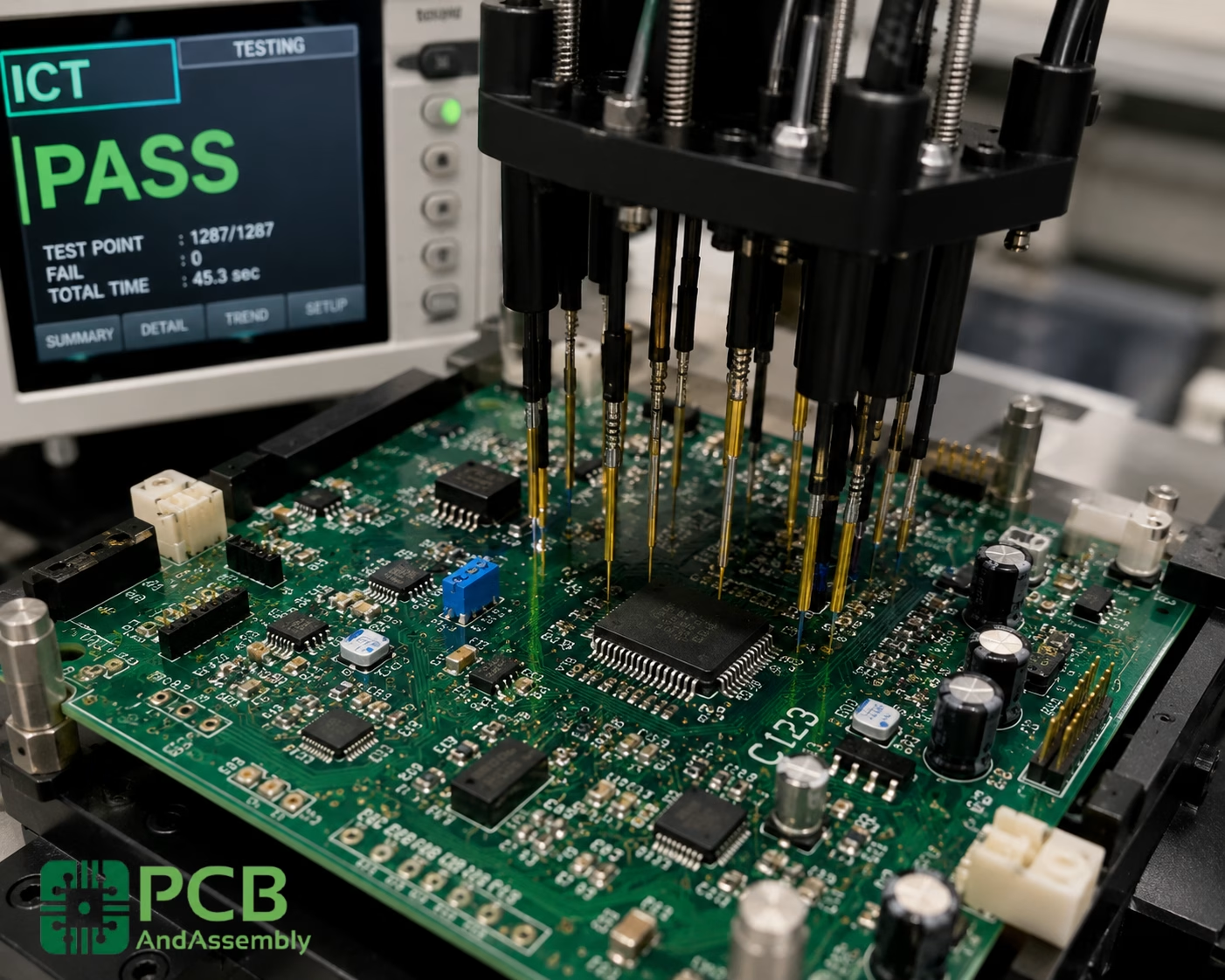
In-Circuit Testing is an automated electrical structural test performed on a fully populated PCB. Rather than treating the board as a single functional unit, ICT treats it as a collection of individual components. Using a bed-of-nails fixture or flying probes, the tester gains direct access to specific nodes and measures resistance, capacitance, inductance, and semiconductor junction characteristics.
The primary objective is to verify that the assembly process was executed correctly: confirming that the right components are installed in the right locations, with correct orientation, and that solder joints provide a low-resistance electrical path. Because ICT targets individual components rather than system behavior, it can isolate a fault down to a specific net or component designator — dramatically reducing rework time and diagnostic effort.
ICT is typically performed unpowered to protect against damage from dead shorts. However, powered ICT is also common for checking voltage regulators or programming onboard flash. The system compares live measurements against a known-good reference board or a netlist derived from CAD data. Measurements falling outside the programmed tolerance — typically 1%–5% — flag the board for repair.
Need PCB Manufacturing or Assembly?
Get a free quote within 24 hours. We specialize in prototype-to-production PCB/PCBA for hardware teams worldwide.
How the ICT Test Cycle Works
Understanding the test sequence helps engineers diagnose failures and optimize program development:
- Board Loading: The PCB is placed on the fixture, manually or via automated handler.
- Fixture Engagement: The bed-of-nails presses against designated test points, establishing electrical contact.
- Component Isolation: Guarding techniques electrically isolate individual components from surrounding circuitry.
- Measurement: The system applies test signals and captures component responses.
- Pass/Fail Determination: Results are compared to programmed limits; out-of-spec boards are flagged.
- Data Logging: All results are recorded for yield tracking and SPC analysis.
The Physics of Guarding: Eliminating Parallel Path Errors
The most common question from junior engineers: “How do you accurately measure one resistor when it is part of a dense, interconnected circuit?” With a standard multimeter, measurement current flows through every available parallel path, producing a false reading. ICT resolves this with a technique called Guarding.
Guarding employs a three-terminal (or six-wire) measurement configuration. The ICT system applies a voltage to the component under test while simultaneously driving surrounding “leakage” nodes to the same potential. With no potential difference between the test node and the guarded nodes, no current flows through the parallel paths — the tester measures only the current through the target component.
A Practical Guarding Example
Imagine a 10 kΩ resistor in parallel with two 5 kΩ resistors connected in series. Without guarding, the meter reads 5 kΩ — the equivalent of the parallel network. By driving the midpoint of the two 5 kΩ resistors to the same voltage as the measurement probe, the ICT system effectively removes those paths from the circuit. This technique enables accurate measurement of a 100 kΩ resistor even when it is shunted by a 10 Ω load elsewhere in the network.
Precision guarding capability is what separates enterprise-grade ICT platforms from budget solutions. Inadequate guarding produces “measurement drift,” causing valid boards to be rejected because parallel paths were not properly suppressed.
Bed-of-Nails vs. Flying Probe: Making the Right Investment
Choosing between a fixed-fixture ICT system and a flying probe tester affects capital expenditure, production throughput, and design flexibility. The right choice follows a break-even analysis of volume versus setup cost.
| Feature | Bed-of-Nails ICT | Flying Probe Testing |
| Initial Setup Cost | High ($5k–$50k+ per fixture) | Low (software programming only) |
| Test Speed | Extremely fast (5–30 sec per board) | Slow (1–15 min per board) |
| Volume Suitability | Mass production (>5,000 units/yr) | Prototypes & low volume (<1,000 units) |
| Design Flexibility | Poor (new fixture per PCB revision) | High (instant software update) |
| Test Coverage | Comprehensive (near 100% nodal access) | Limited by probe count (typically 4–8) |
| NRE Cost | High | Low |
For stable, high-volume designs exceeding 1,000 units per run, a bed-of-nails fixture recovers its cost through reduced cycle time and labor. For rapid-iteration prototyping or high-mix / low-volume (HMLV) environments, the flying probe wins outright. A common and costly mistake is investing in hard fixtures for products that undergo three or more PCB revisions within six months — in those cases, flying probe should remain the method of choice until the design is frozen.
Many manufacturers adopt a hybrid lifecycle strategy: flying probe for New Product Introduction (NPI) and early ramp, then transitioning to a bed-of-nails fixture once the design is stable and volumes justify the investment.
Design for In-Circuit Testing (DFT): The Foundation of Yield
Every ICT failure mode ultimately traces back to decisions made during PCB layout. Boards designed without ICT in mind create structural testing problems that no amount of programming or fixture refinement can fully overcome.
Test Point Requirements
Test points are the physical interface between the fixture and the circuit. Every net requiring verification must have an accessible contact point.
| Parameter | Recommended Value | Absolute Minimum |
| Pad Diameter | 1.0 mm (40 mils) | 0.8 mm (32 mils) |
| Center-to-Center Spacing | 2.54 mm (100 mils) | 1.27 mm (50 mils) |
| Distance from Components | 1.27 mm (50 mils) | 0.64 mm (25 mils) |
| Distance from Board Edge | 3.0 mm (118 mils) | 2.0 mm (79 mils) |
| Surface Finish | ENIG (preferred) | HASL or OSP |
Pushing probe pads below 0.5 mm results in unacceptable probe-miss rates due to fixture tolerances and board thermal expansion. Clustering test points in one corner causes uneven fixture pressure, which can crack ceramic capacitors or crater BGA pads.
The Golden Rules of ICT Layout
Probe Spacing: Maintain at least 1.27 mm (50 mil) center-to-center. Dropping to 0.9 mm requires precision pogo pins that are expensive and fragile.
Distribution: Spread test points evenly across the board surface. Uneven distribution creates localized bending forces during fixture engagement.
Surface Finish: ENIG (Electroless Nickel Immersion Gold) provides the most consistent probe contact. OSP can develop a non-conductive oxide layer over time, producing false “open” failures if probe tips are not sharp enough to pierce the coating.
Critical Nets: Always include test points on power rails, ground nodes, clock lines, reset signals, communication buses, and analog signal paths. Missing even one power rail test point can cascade into missed component failures downstream.
BGA Breakouts: Add test vias on the first via after each critical BGA ball. Without breakout access, vectorless techniques become the only option for detecting open joints.
Common DFT Mistakes That Kill Yield
- Insufficient test point count: Targeting less than 90% net coverage guarantees defect escapes.
- Via-in-pad without compensating probe strategy: Component pads used as test points risk damage from probe tip contact.
- Mixed surface finishes on the same side: Requires multiple probe tip styles and complicates fixture design.
- No distributed ground access: Ground plane connectivity is essential for guarding; isolated ground test points leave entire sections untestable.
- Test points on bottom side only: Forces single-sided probing and limits coverage on dense multi-layer assemblies.
How Fixture Stress Induces Board Warpage and Component Fractures
One of the most insidious failure modes in PCB assembly occurs during the test itself. When a bed-of-nails fixture engages, it applies hundreds of pounds of distributed force to the PCB. Without adequate support, the board flexes — and this flexure is the primary mechanism behind cracked MLCCs (Multi-Layer Ceramic Capacitors) and BGA pad cratering.
Boards thinner than 1.6 mm are particularly susceptible. During fixture development, performing a Strain Gauge Test is strongly recommended. Attaching strain gauges to a sample PCB and logging microstrain during the ICT press cycle reveals bending hot spots. If the measured strain exceeds 500–800 microstrain (depending on component type), additional support pins must be added to the fixture.
Ignoring strain data produces “walking defects” — boards that pass ICT but fail days or weeks later in the field because a hairline crack in a capacitor body finally propagates to a short circuit. These defects are notoriously difficult to trace back to the test process because the board appears electrically sound at the time of test.
Practical recommendation: For PCBs with BGAs larger than 35 mm × 35 mm, or with 0402 and smaller MLCCs within 10 mm of the board center, conduct a strain survey before releasing the fixture to production.
Vectorless Test Techniques for High-Pin-Count ICs
A 1,000-pin BGA typically cannot provide 1,000 physical test points. Vectorless testing — trademarked as TestJet by Keysight and VTEP by Teradyne — bridges this gap without requiring full nodal access.
Vectorless testing works by placing a capacitive sensor plate above the component. The ICT system drives an AC signal through the PCB traces to the IC’s lead frame. The sensor plate measures the resulting capacitance between the lead frame and the plate. An unsoldered pin — an open solder joint — produces a measurably lower capacitance signature than a properly bonded pin. This technique is the most effective method for detecting hidden opens on high-pin-count connectors, BGA devices, and fine-pitch QFP components without requiring extensive nodal access.
Defect Detection Capability by Method
| Defect Type | ICT (Unpowered) | ICT (Powered/Vectorless) | Detection Probability |
| Solder Bridge (Short) | Yes | Yes | >99% |
| Missing Component | Yes | Yes | >99% |
| Wrong Component Value | Yes | No | 95% (tolerances apply) |
| Reversed Polarity (Diode/Tant) | Yes | No | ~90% |
| BGA Open (Cold Solder) | No | Yes (Vectorless) | ~85% |
| Incorrect Firmware | No | Yes (Boundary Scan) | Variable |
| Trace Open | Yes | Yes | >99% |
| Insufficient Solder | Partial | Partial | ~80% |
Boundary Scan Integration: Extending Coverage Beyond Test Points
As component density increases and physical test point real estate shrinks, boundary scan (JTAG / IEEE 1149.1) has become an essential complement to traditional ICT. Modern ICT platforms integrate boundary scan capability directly into the test program, enabling hybrid strategies that achieve coverage levels impossible with either method alone.
ICT probes access the JTAG port pins on the PCB; the boundary scan controller then communicates with all IEEE 1149.1-compliant devices in the chain. This allows the test system to verify interconnect continuity between devices, confirm device identity via manufacturer ID registers, and detect opens on nets that have no physical probe access.
The most practical application is on BGA-heavy designs: ICT handles all accessible discrete and passive components while boundary scan handles the digital ICs, confirming that every net between devices has continuity — even when the only physical access is through the JTAG header.
Comparing ICT, Functional Testing (FCT), and AOI
A robust quality strategy is always multi-layered. No single test method is a silver bullet. Understanding the complementary role of each method prevents both under-testing (defect escapes) and over-testing (inflated costs).
| Factor | AOI | ICT | Functional Test (FCT) |
| Tests Individual Components | Limited | Yes | No |
| Tests System Function | No | Limited | Yes |
| Detects Wrong Values | No | Yes | Indirectly |
| Identifies Root Cause | Visual only | Directly (net/component) | Requires troubleshooting |
| Speed | Fast | Moderate | Slow |
| Setup Cost | Moderate | High | High |
| Best Deployment Stage | Post-reflow | Post-assembly | End-of-line |
The most common yield-destroying mistake is skipping ICT to reduce cost and relying on AOI followed by FCT. Functional testers are effective at confirming that a board works, but they are poor diagnostic instruments. An FCT may report “Communication Error” on a board where Resistor R42 reads 100 Ω instead of 100 kΩ. Manually tracing that error to the correct component consumes more engineer-hours than an ICT fixture would have cost — and allows defects to accumulate before they are caught.
ICT Program Development and Test Limit Optimization
A well-written test program is as important as the fixture itself. Incorrectly set limits produce two types of harm: overly tight limits generate false failures that erode operator confidence; overly loose limits allow real defects to escape.
Setting Appropriate Test Limits
| Component Type | Typical Tolerance | Suggested ICT Limit |
| Resistors (1%) | ±1% | ±3% |
| Resistors (5%) | ±5% | ±10% |
| Ceramic Capacitors (X7R) | ±20% | ±30% |
| Electrolytic Capacitors | -20% / +80% | -25% / +100% |
| Inductors | ±10% | ±15% |
These limits account for component tolerance stacking plus measurement system uncertainty. Tighten limits only when defect data from production provides statistical justification — not based on intuition.
Program Development Phases
- Phase 1 — Data Import: Load CAD netlist, BOM, and Gerber data into the ICT software. Verify net names against the schematic before proceeding.
- Phase 2 — Fixture Design: Generate drilling files from test point coordinates, incorporating probe clearances and board support requirements.
- Phase 3 — Test Generation: The ICT software auto-generates opens, shorts, and component value tests from the BOM. Review auto-generated limits before accepting defaults.
- Phase 4 — Optimization: Run the program on known-good boards and adjust marginal measurements. Flag any test consistently near its threshold for limit review.
- Phase 5 — Debug and Validation: Introduce boards with intentional defects (tombstoned components, wrong-value substitutions) to verify detection.
- Phase 6 — Production Release: Document all limits, guard configurations, and known-marginal tests. Train operators on failure response procedures.
Fixture Maintenance: Preventing Yield Degradation Over Time
Even a perfectly designed fixture degrades. Probe tips wear, spring force decreases, and harness wiring develops intermittent faults. A disciplined maintenance schedule is the difference between a stable yield and a slow, unexplained drift toward higher first-pass failure rates.
| Frequency | Maintenance Action |
| Daily | Visual inspection for visibly damaged or bent probes |
| Weekly | Clean probe tips with approved solvents; remove flux and oxide deposits |
| Monthly | Verify probe travel distance; replace probes below minimum spring force spec; check alignment registration |
| Quarterly | Full fixture calibration; verify all harness connections for continuity; update alignment documentation |
| Per 500k cycles | Comprehensive probe plate inspection; replace all probes regardless of visual condition |
A probe that has lost spring force will intermittently fail to make reliable contact, producing a pattern of “intermittent open” failures that are difficult to distinguish from genuine solder joint defects. Tracking probe hit count per position enables predictive replacement before this failure mode appears.
Treating ICT Data as a Process Control Tool
The defect data generated by ICT is one of the highest-value outputs of the test process — yet many manufacturers treat it as a pass/fail gate rather than a process signal. Analyzing ICT failure logs systematically turns test data into actionable intelligence.
- Track first-pass yield (FPY) by production shift, assembly line, and product family to reveal process drift.
- Monitor component-level failure rates by supplier part number to detect incoming quality degradation before it reaches critical levels.
- A sudden spike in “wrong value” failures on a specific component designator is almost always a feeder loading error or a supplier substitution — catching it through ICT data prevents hundreds of defective boards from advancing to functional test.
- Correlate ICT failure modes with field return data to calibrate test limits: if a certain failure mode appears at ICT but never in field returns, the limit may be too aggressive.
- Use statistical process control (SPC) charts on ICT measurement data — not just pass/fail — to detect drift in component values before the drift crosses the limit threshold.
Troubleshooting Common ICT Problems
High False Failure Rate
False failures are the most common complaint about ICT and usually indicate one of the following:
- Test limits tighter than the combination of component tolerance plus measurement uncertainty.
- Worn or contaminated probe tips producing inconsistent contact resistance.
- Inadequate guarding — parallel circuit paths not sufficiently suppressed during measurement.
- Environmental sensitivity: temperature or humidity affecting measurement baselines.
Defect Escapes Passing ICT
- Insufficient net coverage: critical nets lack test point access.
- Wrong test type applied: using a resistance test where a capacitance or leakage test is required.
- Limits set too wide: tolerances permit marginally defective components to pass.
- Guarding misconfiguration: adjacent components interfering with the measurement path.
Inconsistent Results on the Same Board
- Probe wear causing intermittent contact — identify by correlating failure position with probe hit-count data.
- Fixture alignment drift — verify registration marks monthly.
- Harness wiring breaks or high-resistance crimps — perform periodic harness continuity verification.
Frequently Asked Questions
Can ICT detect cold solder joints?
Partially. ICT reliably detects a true open (no electrical connection). It can also flag a marginal cold joint if the joint’s resistance is high enough to exceed the test limit. However, a cold joint with borderline electrical contact may pass ICT and fail mechanically under vibration or thermal cycling. For verifying mechanical joint integrity on hidden connections, AXI (Automated X-Ray Inspection) is superior.
What is the difference between ICT and Boundary Scan (JTAG)?
ICT requires a physical probe to contact every net it tests. Boundary Scan (JTAG / IEEE 1149.1) uses built-in logic within compliant ICs to toggle output pins and sense input pins without any physical probe contact. The two methods are complementary: ICT tests passives and nets with physical access; boundary scan extends coverage to digital ICs and nets that lack test points. Modern ICT systems integrate both within a single test program.
Does ICT damage components?
When programmed and maintained correctly, ICT is safe. Unpowered tests use voltages below 0.5 V with current limiting, ensuring semiconductor junctions are never stressed. Physical probe pressure is the more realistic risk — a misaligned fixture or excessive probe force can damage fine-pitch pads. Strain gauge testing and regular fixture calibration mitigate this risk.
Why is my ICT yield lower than my functional test yield?
This typically indicates over-tight tolerances in the ICT program relative to actual component specifications. If ICT is programmed to 1% limits but the bill of materials specifies 5% tolerance components, legitimate boards will be rejected as failures. Review the guard configurations and compare programmed limits against the component data sheets. A false reject rate above 0.5–1% warrants immediate investigation.
When does ICT become economically justified?
The crossover point depends on assembly complexity, but a practical rule of thumb: for stable designs producing more than 500–1,000 boards per year, the throughput gain from a bed-of-nails fixture typically recovers fixture costs within the first production lot. For volumes below this threshold, flying probe or outsourced ICT is more cost-effective.
Implementation Roadmap
| Annual Volume | Recommended Approach |
| Under 500 boards | Flying probe or outsourced ICT — no fixture investment justified |
| 500–5,000 boards | Shared fixture strategy or contract test house with dedicated fixtures |
| 5,000–50,000 boards | Dedicated fixtures; consider owned equipment vs. outsourced by TCO |
| Over 50,000 boards | In-house ICT system with dedicated fixtures and full DFT process |
For teams implementing ICT for the first time, a ten-week timeline is realistic: weeks 1–2 for equipment or test service selection; weeks 3–4 for DFT review and PCB layout updates; weeks 5–6 for fixture order and program development; weeks 7–8 for prototype board debugging; weeks 9–10 for pilot production validation; week 11 onward for production release and continuous optimization.
Summary
In-Circuit Testing remains the most reliable structural electrical verification method available to PCB assembly manufacturers. Through component isolation via guarding and direct nodal access, it delivers diagnostic precision that neither AOI nor functional testing can match at production speed. Its effectiveness, however, is entirely contingent on decisions made long before the first board reaches the fixture.
As a practitioner, my recommendation is this: never treat ICT as an afterthought. If you wait until the design is “done” to think about test points, you will pay for it in fixture complexity and reduced yield. Involve your test engineer at the schematic stage. Ensure that your PCB laminate can handle the strain, and always—always—validate your first-run fixtures with strain gauges if you are using large, fine-pitch BGA components.
