IoT PCB Assembly Everything You Need to Know
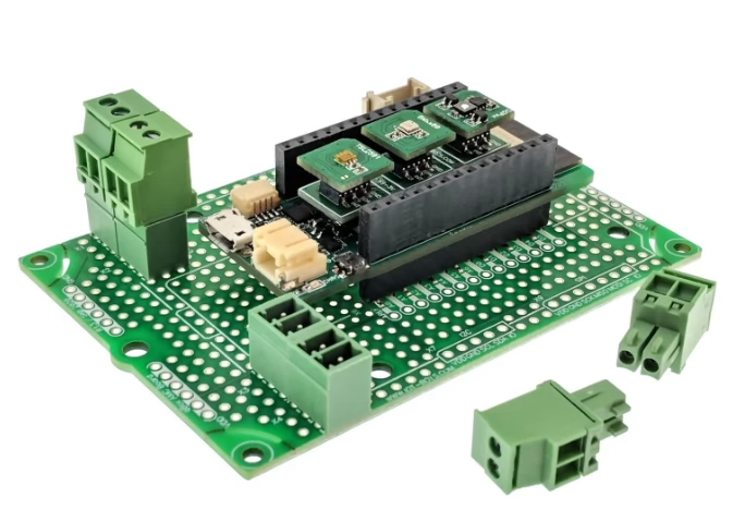
From smart home devices to industrial sensors and wearables — we deliver precision IoT PCB assembly built for connectivity, low-power operation, and long-term reliability.
Our experienced team handles RF design, HDI boards, wireless module integration, and full turnkey assembly under one roof.
What Is an IoT PCB?
An IoT PCB (Internet of Things Printed Circuit Board) is a specialized circuit board designed to enable smart, connected devices. Unlike conventional PCBs that simply provide electrical connections between components, IoT PCBs integrate sensors, wireless communication modules, microcontrollers, and power management systems — all optimized for network connectivity and data exchange.
Think of it this way: a traditional PCB is like a standalone calculator. An IoT PCB is more like a smartphone — it is not just processing information locally but constantly communicating with the outside world.
IoT PCB design comes with challenges you simply do not encounter in traditional board work. You are balancing wireless performance, battery life, thermal constraints, and security — all in a smaller package. The Internet of Things has fundamentally changed how we approach printed circuit board design. We are no longer just routing traces and placing components; we are building the nervous system of an interconnected world.
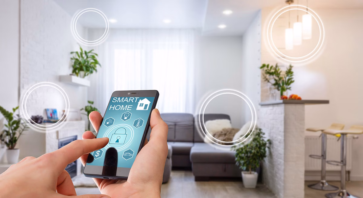
From the smart thermostat in your living room to industrial sensors monitoring factory equipment 24/7, IoT PCBs are everywhere — and they demand a different mindset.
Key Characteristics of IoT PCBs
- Compact Form Factor — HDI & miniaturization
- Wireless Connectivity — Wi-Fi, BLE, LoRa, Zigbee
- Low Power Operation — Months on a single battery
- Sensor Integration — Environmental & motion data
- Hardware Security — Encryption & secure boot
IoT PCB Assembly Capabilities
We support every stage of IoT PCB production — from schematic review and DFM analysis to full turnkey assembly, RF testing, and regulatory compliance support.
Wireless Protocol Comparison
Choosing the right wireless protocol is one of the most critical decisions in IoT PCB design. Each has trade-offs in terms of range, power consumption, data rate, and complexity.
| Protocol | Range | Data Rate | Power Consumption | Best For |
| Wi-Fi | 50–100 m | Up to 1 Gbps | High | High-bandwidth, always-powered devices |
| Bluetooth LE | 10–100 m | 1–2 Mbps | Low | Wearables, proximity sensing |
| Zigbee | 10–100 m | 250 Kbps | Very Low | Smart home, mesh networks |
| LoRa | 2–15 km | 0.3–50 Kbps | Very Low | Long-range sensors, agriculture |
| NB-IoT | Cellular | 250 Kbps | Low | Wide-area IoT, remote monitoring |
| Thread | 10–100 m | 250 Kbps | Low | Smart home, Matter ecosystem |
| Wi-Fi HaLow (802.11ah) | Up to 1 km | 150 Kbps–78 Mbps | Moderate | Smart buildings, outdoor IoT |
IoT PCB Substrate Materials
Material selection impacts everything from signal integrity to long-term reliability. Here is a breakdown of the most common materials for IoT applications.
Most Common: FR-4 — The Workhorse
Cost-effective, widely available, and works well for most IoT applications. Dielectric constant around 4.0–4.4, operating temperature up to 130–140°C. Ideal for smart home devices, fixed industrial sensors, and most general IoT products.
Flexible: Polyimide — When Flexibility Matters
The go-to for flexible and rigid-flex PCBs. Dielectric constant 3.2–3.5, operating temperature up to 260–300°C. Perfect for wearables, medical implants, and any application where the board needs to bend, fold, or conform to curved surfaces.
High-Frequency RF: Rogers / PTFE — RF Performance
Rogers RO4350B and PTFE (Teflon) materials offer lower dielectric constant and loss tangent — crucial for 2.4 GHz Wi-Fi, 5 GHz bands, and cellular IoT. Often used in hybrid stackups alongside FR-4 for the RF section only.
Extreme Environments: Ceramic — Extreme Thermal
Aluminum nitride or alumina substrates for extremely high thermal loads and harsh environments. Used in high-power LED drivers, automotive IoT modules, and applications demanding exceptional thermal conductivity and long-term reliability.
| Property | FR-4 | Polyimide |
| Flexibility | Rigid | Highly flexible |
| Dielectric Constant (Dk) | 4.0–4.4 | 3.2–3.5 |
| Max Operating Temp | 130–140°C | 260–300°C |
| Cost | Lower | Higher |
| Moisture Absorption | 0.1% | Up to 2% |
| Typical Thickness | 0.8–1.6 mm | 0.05–0.3 mm |
| Best Applications | General IoT, fixed installations | Wearables, medical devices, space-constrained designs |
IoT PCB Applications Across Industries
Smart Home Devices
Thermostats, lighting controllers, security cameras, and voice assistants. Typically wall-powered, prioritizing Wi-Fi or Bluetooth connectivity and cost-competitive form factors.

Industrial IoT
Factory automation, predictive maintenance, and process monitoring. Wide temperature ranges (−40°C to +85°C), vibration resistance, 10+ year operational lifetimes, and conformal coating as standard.

Wearable Technology
Fitness trackers, smartwatches, and medical wearables. Extreme miniaturization using HDI and flex PCBs, very low power, and biocompatibility for skin-contact devices.

Healthcare & Medical IoT
Medical-grade IoT devices with FDA / IEC 60601 compliance, patient safety and data security requirements, and precision sensing for accurate health monitoring.

Agricultural IoT
Soil sensors, crop health monitors, and livestock trackers. Years of battery life, extreme weather resistance, and long-range LoRa / NB-IoT connectivity for large-area deployments.
Automotive & Transportation
Fleet tracking, in-vehicle sensors, and EV monitoring systems. AEC-Q100 qualified component support, wide temperature range, and EMC-hardened designs for vehicle environments.
How to Order Your Industrial Control PCB Assembly
IoT PCB Design Best Practices
After working on hundreds of IoT projects, our engineering team has compiled the practices that consistently lead to successful, first-pass designs.
Group by Function
Keep analog circuits separate from digital, RF sections isolated, and power components together. This is about signal integrity and EMI control, not just convenience.
Prioritize the RF Path
The antenna and RF frontend should drive placement decisions. RF traces need to be as short as possible with controlled impedance. Follow your module manufacturer’s reference design exactly.
Design for Low Power from Day One
Calculate your power consumption in every operating state. Use deep sleep modes, efficient DC-DC converters, and power gating for unused peripherals.
Tackle EMI/EMC Early
A solid ground plane, proper filtering between functional blocks, series termination on clocks, and RF shielding cans prevent expensive certification failures later.
Plan for Testability
Include test points for critical signals, power rails, and communication buses. You will thank yourself during bring-up and production test.
Respect Thermal Budgets
Distribute heat sources across the board, use thermal vias under hot components, and calculate thermal margins during design — not after you have a problem in the field.
Security is Hardware-Level
Secure elements for key storage, secure boot, debug port protection, and physical tamper detection should all be designed in from the start — not bolted on later.
Design for Manufacturing (DFM)
Use standard via sizes and trace widths, provide adequate clearance for pick-and-place machines, include fiducials for optical alignment, and design panel utilization thoughtfully.
IoT PCB Assembly FAQs
What makes IoT PCB design different from regular PCB design?
IoT PCB design adds several layers of complexity beyond traditional board work. You are integrating wireless connectivity, which introduces RF design challenges and antenna considerations. Power management becomes critical since many IoT devices run on batteries for extended periods. Form factors are often smaller, requiring HDI techniques. And you must consider security at the hardware level since these devices connect to networks. In traditional PCB design, you might route some signals and call it done. In IoT, you are balancing wireless performance, battery life, thermal constraints, and security — all in a smaller package.
How do I choose between FR-4 and polyimide for my IoT PCB?
Use FR-4 when your device is in a fixed form factor, operates in moderate temperatures (below 130°C), and cost is a primary concern. Choose polyimide when you need flexibility (wearables, medical devices that conform to body shapes), high-temperature operation (above 150°C), or very thin boards. For many IoT projects, standard FR-4 works fine. But if your device needs to bend, survive extreme heat, or fit into unusual shapes, polyimide is worth the additional cost.
How many layers should my IoT PCB have?
For simple IoT devices with basic connectivity (like a Bluetooth sensor node), you might manage with 2 layers, though 4 is more comfortable. For Wi-Fi devices or anything with significant digital complexity, 4–6 layers is typical. High-performance designs with multiple RF paths, complex power management, or high-speed interfaces often need 6–8 layers or more. The decision comes down to routing density, signal integrity requirements, and EMI management. More layers cost more, but trying to squeeze a complex design into too few layers often ends up costing more through redesigns and EMI failures.
What certifications do IoT PCBs need?
In the United States, any IoT device with wireless functionality needs FCC certification. In Europe, CE marking is required. Other regions have their own requirements (IC for Canada, MIC for Japan, etc.). Depending on your application, you may also need UL safety certification, RoHS compliance, medical device certifications (FDA, IEC 60601), or automotive certifications (AEC-Q100). Build these requirements into your design process from the start — retrofitting compliance is expensive and often requires board respins. We provide pre-certification DFM checks and can refer you to accredited test labs.
What are the most common causes of IoT PCB failures?
The top failure modes are: poor antenna performance due to bad placement or inadequate ground plane design; thermal issues from underestimating heat generation in compact enclosures; power supply problems including excessive noise or inadequate decoupling; ESD damage from insufficient protection on exposed interfaces; and solder joint failures in products subjected to thermal cycling or vibration. Most of these are preventable with proper upfront design attention. The key is optimizing not just for initial function but for long-term reliability in real operating conditions.
Can you assemble both SMT and THT on the same IoT board?
Yes. We offer mixed-technology assembly combining SMT reflow and selective or wave soldering for through-hole components. Most IoT boards are predominantly SMT, but connectors, antennas, and some power components often require through-hole mounting. We support both in a single production flow.
Do you support IoT 4.0 and digital transformation projects?
Absolutely. We work with companies integrating IIoT into their existing infrastructure, including smart factory sensor nodes, gateway devices, predictive maintenance boards, and cloud-connected data acquisition units. We understand the requirements for industrial communication protocols, wide operating temperature ranges, and the extended product lifespans that Industry 4.0 deployments demand.
Need PCB Manufacturing or Assembly?
Get a free quote within 24 hours. We specialize in prototype-to-production PCB/PCBA for hardware teams worldwide.