Communication PCB Assembly services
PCBAndAssembly a complete integrated solution from design and engineering support, to production and full system assembly.
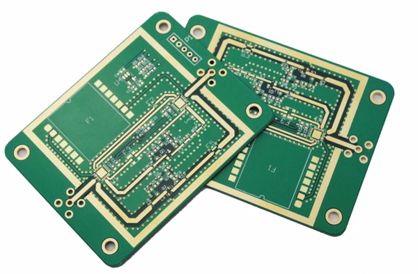
Professional communication PCB assembly one-stop service provider specializing in high-frequency, high-performance 4G/5G circuit boards.
Features 6-layer FR-4 PCBs, 0.2mm min. hole size, ENIG/Immersion Silver finishes, and 100% electronic testing. Custom solutions, fast delivery—your trusted communication PCB partner.
What Is an Communication PCB?
In the field of communications, communication PCB boards play a crucial role in various applications such as wireless networks, transmission networks, data communications, and fixed-line broadband. These PCB boards encompass a range of products including backplanes, high-speed multilayer boards, high-frequency microwave boards, HDI boards and multi-function metal substrates.
PCB requirements in the communications field are divided into subdivisions such as communication devices and mobile terminals. Communication equipment is mainly used for communication infrastructure for wired or wireless network transmission. Including communication base stations, routers, switches, etc. Communication equipment mainly uses high-layer PCB boards, of which 8-16 layers account for about 42%. And mobile terminals are mainly HDI and flexible boards.

Communication PCB Advanced Manufacturing Capabilities
We have an experienced team of communication PCB design engineers and modern production lines capable of handling various communication PCB assembly needs—from simple single-layer boards to complex multilayer designs. Our technical strengths include:
High-Frequency Design Expertise
Proficient in microwave band (700MHz–5GHz) circuit design for optimal 5G device performance.
Precision Machining
Minimum aperture of 0.2mm, trace width/spacing of 4–6 mil, supporting high-density interconnects.
Multiple Surface Finishes
Options include HASL (Lead-Free), ENIG (Immersion Gold), OSP, and Immersion Silver.
Strict Quality Control:
Full-process quality monitoring from raw materials to finished products.
Communication PCB 5G construction features
Communication PCBs in 5G construction have significant features and requirements due to the high-speed and high-frequency nature of 5G technology. These features drive the demand for communication boards, especially in the construction of 5G base stations.
Increased Base Station Quantity: The number of 5G base stations is much larger compared to current 4G base stations. Additionally, the deployment of micro base stations in blind spot areas further contributes to the demand for communication PCB boards.
Industrial Control Environment: Communication PCBs are utilized in both wired and wireless communication equipment within industrial control environments. Wired communication equipment includes serial communication, professional bus-type communication, industrial Ethernet communication, and various communication protocol conversion equipment. Wireless communication equipment encompasses wireless APs, wireless bridges, wireless network cards, wireless lightning arresters, antennas, and other related devices.
High-Frequency and High-Speed Requirements: The RF (Radio Frequency) part of communication PCBs operates at relatively high frequencies, while the baseband part handles digital signals with very high data rates. These characteristics impose stringent material requirements on the PCBs. Some components may also require boards with ceramic substrates to meet specific performance needs.
Complex PCB Design and Processing: Communication PCBs often have dozens of layers, including through-hole plates. They may require a back-drilling process to ensure precise signal integrity and minimize signal reflection.
Our experienced engineers and state-of-the-art facilities enable us to handle the complex design and processing needs of communication PCBs. With the ability to manufacture multi-layered PCBs with precision and efficiency, including through-hole plates and back-drilling processes, we ensure excellent signal integrity and minimize signal reflection.
Need PCB Manufacturing or Assembly?
Get a free quote within 24 hours. We specialize in prototype-to-production PCB/PCBA for hardware teams worldwide.
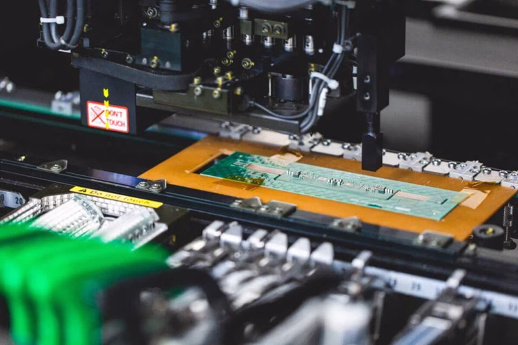
Communication PCB Assembly and Testing Processes
Assembly and testing are crucial to ensuring Communication PCB reliability. At PCBAndAssembly, we perform surface mount technology (SMT) and through-hole assembly using IPC Class 3 standards. Our inspection and testing processes include AOI, X-ray inspection, in-circuit testing (ICT), and functional testing. We also offer flying probe and environmental stress screening (ESS) to simulate real-world operating conditions. These steps ensure each Communication PCB meets stringent quality and performance benchmarks.
Communication PCB Applications

Communication Infrastructure
- Cell Transmission and Tower Electronics
- Fixed & Mobile Networks
- Satellite Technology
- Wireless Industrial and Commercial Phone Technology
- Broadband Equipment
- Fiber Optic Communication

Data Transmission and Networking
- High-Speed Routers and Switches
- Server Systems
- Data Centers
- Network Switching Equipment
- Broadband Modems
- Ethernet Devices
Security and Encryption
- Information Security Technology
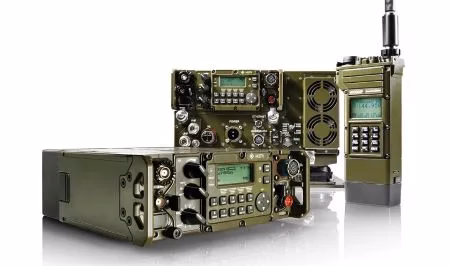
- Military Communications Systems
- Encryption Devices
- Secure Communication Systems
- Network Firewalls

Voice and Video Communication
- PBX Systems
- Voice over IP (VoIP) Devices
- Video Conferencing Systems
- Unified Communication Systems
- Audio/Video Processing Equipment
- Intercom Systems

Specialized Applications
- Waveguide Grating Devices
- Signal Amplification Devices
- Airbag Deployment Systems
- Industrial Control Systems
- Sensing and Monitoring Equipment
- Medical Communication Devices

Consumer Electronics
- Smartphones and Tablets
- Internet of Things (IoT) Devices
- Home Networking Equipment
- Audio/Video Entertainment Systems
- Wearable Devices
- Gaming Consoles