1 oz PCB: Complete Guide to Standard Copper Weight for General-Purpose & High-Volume Designs
The 1 oz PCB (35 µm thick per layer) has been the industry-standard copper weight for decades. It carries enough current for most digital and analog circuits, supports reliable solder joints for standard surface-mount components, and can be etched with sufficient precision for trace widths down to 4-5 mils. It's the copper weight that billions of boards are built to each year.
Get Your PCB Quote!
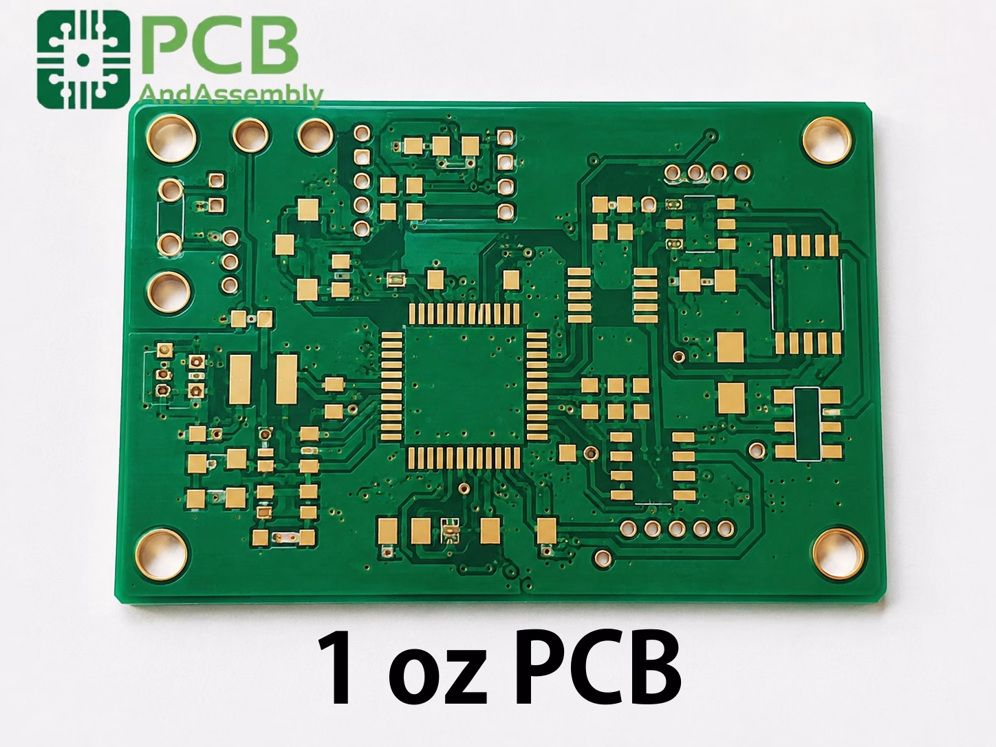
Table of Contents
Table of Contents
1 oz copper is the default choice for PCB fabrication — and for good reason. It offers an optimal balance of current capacity, signal integrity, manufacturability, and cost that works for the vast majority of designs. When you send a board out for quote without specifying copper weight, 1 oz is what you’ll get back. When you open a datasheet for a standard FR-4 laminate, 1 oz is the baseline. When every quick-turn prototype shop advertises its standard lead time, that’s for 1 oz copper.
What is 1 oz PCB?
A 1 oz PCB uses copper foil weighing one ounce per square foot on each conductive layer. This is the PCB industry’s baseline specification — the default that every fabricator stocks and every designer works from unless a specific reason exists to deviate.
The “ounce” convention dates back to the early days of PCB manufacturing, when copper foil suppliers specified their products by weight per square foot. The convention stuck because it translates directly to ordering: when you specify 1 oz copper at a fab house, there is zero ambiguity about what you’re asking for.
| Copper Weight | Thickness (µm) | Thickness (mils) | Thickness (mm) |
| 0.5 oz | 17.5 | 0.7 | 0.0175 |
| 1 oz (standard) | 35 | 1.37 | 0.035 |
| 2 oz | 70 | 2.74 | 0.070 |
| 3 oz | 105 | 4.11 | 0.105 |
| 4 oz | 140 | 5.48 | 0.140 |
Where 1 oz Fits in the Copper Weight Spectrum
Copper weights range from ultra-thin (0.25 oz, ~9 µm) for specialized flex circuits to heavy copper (10 oz, ~350 µm) for high-current industrial power systems. The 1 oz PCB sits at the center of this spectrum:
| Weight Class | Copper Weight | Typical Applications |
| Ultra-thin | 0.25-0.5 oz | Flex circuits, HDI, RF/microwave |
| Standard | 1 oz | General-purpose PCBs, most designs |
| Medium copper | 2-3 oz | Power supplies, automotive, motor drives |
| Heavy copper | 4-10 oz | High-current industrial, EV, traction |
1 oz copper occupies the “standard” category — and it’s worth noting that the vast majority of PCB production worldwide uses this weight. It represents the intersection of capability, cost, and manufacturing maturity.
How 1 oz Became the Industry Standard
The dominance of 1 oz copper is not accidental. Several factors converged to make it the default:
Laminate Manufacturing Standardization: When FR-4 became the dominant PCB substrate in the 1970s and 1980s, laminate manufacturers optimized their production lines around 1 oz copper cladding. The material is widely available from multiple suppliers (Isola, Panasonic, Shengyi, Kingboard) with tight tolerances and consistent quality.
Connector and Component Compatibility: Edge connectors, card-edge contacts, and press-fit terminals were designed around 1 oz copper thickness. The spring force and contact resistance specifications assume this copper weight, and deviating can cause reliability issues with standard connectors.
Solder Joint Reliability: Standard SMT and through-hole solder processes were developed around 1 oz copper’s thermal characteristics. The copper provides adequate heat spreading for soldering while being thin enough for proper reflow profiles.
Manufacturing Economics: Fabricators process 1 oz copper more efficiently than alternative weights. Etching times, drilling parameters, and handling equipment are all optimized for this standard. The per-square-foot cost of 1 oz copper is the lowest of any weight due to economies of scale.
1 oz PCB Electrical Properties
The 35 µm thickness of 1 oz copper provides electrical characteristics that suit the majority of PCB applications.
Current Carrying Capacity
Current capacity scales directly with copper cross-sectional area. For 1 oz copper at standard temperature rises, the following table shows approximate current-handling capability.
Current Capacity Table (External Layer, Various Temperature Rises):
| Trace Width | 10°C Rise | 20°C Rise | 30°C Rise |
| 5 mil | ~1.0A | ~1.4A | ~1.8A |
| 10 mil | ~2.3A | ~3.2A | ~4.0A |
| 20 mil | ~4.6A | ~6.5A | ~8.2A |
| 50 mil | ~11.0A | ~15.5A | ~19.5A |
| 100 mil | ~22.0A | ~31.0A | ~39.0A |
Note: Values are estimates based on IPC-2152. Internal layer capacity is approximately 50-70% of external due to reduced heat dissipation. Always verify with specific design conditions.
For most digital and analog designs where signal traces carry milliamps of current, a 5-10 mil trace on 1 oz copper provides more than enough capacity. Power distribution traces require wider widths, but for designs up to a few amps, 1 oz copper usually suffices without special design provisions.
Impedance Control
For controlled-impedance designs, 1 oz copper is well-suited for standard trace geometries. A 50 Ω microstrip line on standard FR-4 typically requires trace widths of 8-12 mils depending on the dielectric thickness — perfectly practical for most designs.
Approximate 50 Ω Microstrip Widths (1 oz on FR-4, Dk ~4.2):
| Dielectric Thickness | Trace Width (1 oz) |
| 4 mil (0.1 mm) | ~7.0 mil |
| 8 mil (0.2 mm) | ~15 mil |
| 12 mil (0.3 mm) | ~23 mil |
1 oz copper provides a good balance: the copper is thick enough for low DC resistance in transmission lines but thin enough that etching variations don’t dominate impedance tolerance. Most fabricators can maintain ±10% impedance tolerance on 1 oz copper without special process controls, and ±5% is achievable with TDR verification.
DC Resistance
DC resistance per unit length is approximately half that of 0.5 oz copper at the same trace width. This translates to lower voltage drops in power distribution networks and less resistive heating in signal traces.
| Trace Width | 1 oz Resistance (mΩ/inch) | 0.5 oz Resistance (mΩ/inch) |
| 5 mil | ~48 | ~95 |
| 10 mil | ~24 | ~48 |
| 20 mil | ~12 | ~24 |
| 50 mil | ~4.8 | ~9.5 |
Skin Effect at High Frequencies
At frequencies above 1 GHz, skin effect becomes significant. The skin depth of copper at 1 GHz is approximately 2.1 µm, and at 10 GHz it’s about 0.66 µm. Since 1 oz copper is 35 µm thick — far thicker than the skin depth at these frequencies — the skin effect resistance is dominated by surface roughness rather than copper thickness itself.
For designs up to approximately 5-10 GHz, 1 oz copper performs adequately. Above that frequency range, the surface roughness of standard ED copper foil becomes the dominant loss mechanism, and smooth foils (RTF, VLP) or thinner copper weights may be preferred.
Advantages and Disadvantages of 1 oz PCB
Advantages
Industry Standard Availability: 1 oz copper is stocked by every laminate manufacturer and PCB fabricator worldwide. There are no minimum order quantities, no specialty material surcharges, and no lead time penalties. When you design with 1 oz, you have the entire global PCB supply chain at your disposal.
Excellent Balance of Properties: 1 oz copper provides adequate current capacity for most designs, sufficient mechanical strength for reliable solder joints, good thermal spreading, and fine enough etching resolution for standard pitch components (down to 0.5 mm BGA pitch).
Lowest Cost Per Square Foot: Because 1 oz is produced in the highest volumes, it has the lowest material cost per square foot of any copper weight. Combined with the fastest fabrication times (no special etching or drilling processes needed), 1 oz boards are consistently the most economical option.
Best Turnaround Time: Quick-turn PCB services — whether 24-hour, 48-hour, or 5-day — all default to 1 oz copper. If your design requires a non-standard weight, lead times typically increase by 2-5 days.
Proven Reliability: 1 oz copper’s thermal and mechanical characteristics in PCB assemblies are thoroughly understood and modeled. Solder joint reliability models, thermal cycling life predictions, and via reliability calculations all have extensive validation data for 1 oz copper.
Fine-Pitch Compatibility: 1 oz copper supports trace widths down to 4-5 mils with standard etching, which is sufficient for most component pitches down to 0.4-0.5 mm. This covers the majority of BGAs, QFNs, and fine-pitch connectors used in commercial designs.
Disadvantages
Limited High-Current Capability: At sustained currents above 3-5A per trace, 1 oz copper requires very wide traces (50+ mils) or copper pours. For designs with multiple high-current paths, 2 oz or heavier copper is more practical.
Not Optimized for Ultra-Fine Features: While 4-5 mil traces are achievable, HDI designs with 2-3 mil traces and microvias benefit from 0.5 oz copper, which etches more cleanly and provides better impedance control at very fine geometries.
Heavier Than Necessary for Some Applications: For very small, low-power designs — think wearable sensors, IoT modules, and medical patches — 0.5 oz copper provides adequate electrical performance with less weight and thinner overall construction.
| Parameter | 0.5 oz | 1 oz | Best For |
| Min trace width | 2-3 mils | 4-5 mils | 0.5 oz |
| Current capacity | Lower | Standard | 1 oz |
| Impedance control | Excellent | Good | 0.5 oz |
| Mechanical strength | Lower | Good | 1 oz |
| Availability | Good | Excellent | 1 oz |
| Cost | Slightly lower | Baseline | 1 oz |
| Quick-turn available | Usually | Yes | 1 oz |
| Fine-pitch BGA (< 0.5mm) | Excellent | Moderate | 0.5 oz |
Applications for 1 oz PCB
The versatility of 1 oz copper makes it suitable for an extraordinarily wide range of industries and applications.
Consumer Electronics
Consumer devices represent the largest volume of 1 oz PCB production. Smartphones, tablets, laptops, TVs, gaming consoles, and smart home devices all use 1 oz copper on their main boards.
- Smartphone and tablet main logic boards
- Laptop and desktop motherboards
- Gaming console PCBs
- Smart TV control boards
- Smart home hub and IoT gateway boards
- Set-top boxes and streaming devices
For most consumer electronics, the current requirements are modest (under 2A per trace), and the component pitch is standard enough for 4-5 mil trace/space rules. 1 oz copper provides the right balance of performance and cost for mass production.
Industrial Controls and Automation
Industrial environments demand reliability, and 1 oz copper delivers the mechanical robustness needed for PLCs, motor controllers, and industrial communication modules.
- Programmable logic controller (PLC) boards
- Industrial sensor interface modules
- Motor drive and actuator controller boards
- Factory automation communication gateways
- Power monitoring and metering equipment
The excellent solder joint reliability of 1 oz copper is particularly valuable in industrial applications where vibration and thermal cycling are common.
Automotive Electronics
Modern vehicles contain dozens of PCBs for engine control, infotainment, body control, and driver assistance systems. Automotive-grade materials (high-Tg FR-4) typically use 1 oz copper as the standard.
- Engine control units (ECUs) and transmission controllers
- Infotainment system main boards
- Body control modules (door locks, lighting, windows)
- ADAS sensor interface boards
- Battery management system (BMS) monitor boards
- Interior lighting and comfort control modules
Automotive applications often require thicker copper in specific areas (power stages), but 1 oz remains the standard for signal processing and control sections.
Telecommunications and Networking
Networking equipment — switches, routers, base stations, and fiber optic transceivers — relies heavily on 1 oz copper for its combination of signal integrity and power handling.
- Network switch and router main boards
- Baseband processing units for cellular base stations
- Fiber optic transceiver PCBs
- Ethernet switch interface boards
- Server mainboards and backplanes
For high-speed digital designs operating at 1-25 Gbps, 1 oz copper’s impedance control characteristics are well understood and widely modeled in signal integrity tools.
Medical Devices
Medical electronics range from diagnostic imaging equipment to patient monitoring systems, all of which benefit from the proven reliability of 1 oz copper.
- Patient monitor interface boards
- Diagnostic imaging control electronics (ultrasound, X-ray)
- Ventilator and anesthesia system controllers
- Infusion pump electronics
- Laboratory analysis equipment boards
Medical applications often require IPC Class 2 or Class 3 quality, and 1 oz copper is the standard weight specified in these quality systems.
| Industry | Typical Current | Key Requirements |
| Consumer electronics | < 3A | Low cost, high volume |
| Industrial controls | < 5A | Reliability, vibration resistance |
| Automotive | < 10A (mixed) | Thermal cycling, high-Tg material |
| Telecom/networking | < 3A | Signal integrity, impedance control |
| Medical devices | < 3A | Quality certification, reliability |
1 oz vs 0.5 oz vs 2 oz: How to Choose the Right Copper Weight
The decision matrix is straightforward for most designs: start with 1 oz and deviate only when specific requirements force a change.
Decision Framework
| Design Requirement | Recommended Weight | Reason |
| General-purpose design | 1 oz | Industry standard, lowest cost |
| High-density routing (< 4 mil traces) | 0.5 oz | Better etching resolution |
| High current (> 3A per trace) | 2 oz or heavier | Adequate current capacity |
| Standard BGA (0.5 mm+ pitch) | 1 oz | Sufficient trace breakout |
| Ultra-fine BGA (< 0.4 mm pitch) | 0.5 oz | Enables trace escape routing |
| High-frequency RF (> 10 GHz) | 0.5 oz | Better impedance control, lower surface roughness loss |
| Cost-sensitive > reliability | 1 oz | Most economical |
| Quick-turn prototype | 1 oz | Fastest turnaround available |
| Power supply design | 2 oz | Lower resistance, better thermal |
When 1 oz is the Wrong Choice
Honestly evaluate these scenarios before committing to standard weight:
Scenario 1 — You need to route traces finer than 4 mils. If your design has 0.4 mm or finer BGA pitch requiring 3 mil or narrower traces, 0.5 oz copper will give you better etching precision and higher yield.
Scenario 2 — Your design carries sustained currents over 5A per trace. With 1 oz copper, a 5A trace needs to be approximately 25-30 mils wide (external, 20°C rise). Multiple high-current traces quickly consume board area — 2 oz copper halves the required width.
Scenario 3 — Board thickness must be minimized. For thin products (under 1.0 mm total thickness), 0.5 oz inner layers allow thinner prepreg and core materials.
Scenario 4 — Extreme reliability requirements. In aerospace, defense, or medical life-support applications where thermal cycling and vibration are extreme, 2 oz copper provides additional mechanical margin in plated through-holes and solder joints.
Practical Hybrid Approaches
Many production designs use a mix of copper weights to optimize cost, density, and performance simultaneously.
Example 4-Layer Hybrid Stackup:
| Layer | Function | Copper Weight | Reason |
| L1 (Top) | Signal + components | 1 oz | Component pad reliability |
| L2 | Ground plane | 1 oz | Standard reference plane |
| L3 | Power plane | 1 oz | Current distribution |
| L4 (Bottom) | Signal + components | 1 oz | Component pad reliability |
Example 6-Layer Hybrid with Power Focus:
| Layer | Function | Copper Weight | Reason |
| L1 (Top) | Signal + components | 1 oz | Component pads |
| L2 | Ground plane | 1 oz | Reference plane |
| L3 | Signal (high-density) | 0.5 oz | Fine-line routing |
| L4 | Signal (high-density) | 0.5 oz | Fine-line routing |
| L5 | Power plane | 2 oz | High-current distribution |
| L6 (Bottom) | Signal + components | 1 oz | Component pads |
1 oz PCB Design Guidelines
Designing with 1 oz copper is straightforward because it’s the baseline that PCB CAD tools and fabricators assume. Here are the practical guidelines.
Trace Width and Spacing
For 1 oz copper, most manufacturers specify minimum trace widths and spacing of:
| Feature | Standard Capability | Advanced Capability |
| Min trace width | 5 mil (0.125 mm) | 4 mil (0.1 mm) |
| Min spacing | 5 mil (0.125 mm) | 4 mil (0.1 mm) |
| Min trace width (impedance controlled) | 5 mil (0.125 mm) | 4 mil (0.1 mm) |
At 5/5 mil trace/space rules, 1 oz copper gives you good routing density for most designs. For comparison, the same rule on 0.5 oz copper could be tightened to 3/3 mil — but for the majority of commercial designs, 5/5 mil is adequate.
Impedance Control with 1 oz
1 oz copper provides predictable impedance characteristics that are well-modeled in all major field solvers.
Approximate 50 Ω Microstrip Widths (1 oz):
| Dielectric Thickness | Dielectric Material | Trace Width (1 oz) |
| 4 mil (0.1 mm) | FR-4 (Dk ~4.2) | ~7.0 mil |
| 8 mil (0.2 mm) | FR-4 | ~15 mil |
| 12 mil (0.3 mm) | FR-4 | ~23 mil |
Approximate 100 Ω Differential Microstrip (1 oz, 8 mil dielectric):
| Trace Width | Gap (Edge-to-Edge) | Achieved Zdiff |
| 5 mil | 5 mil | ~95 Ω |
| 5 mil | 8 mil | ~105 Ω |
| 6 mil | 6 mil | ~93 Ω |
| 6 mil | 8 mil | ~100 Ω |
These values are starting points — always verify with your fabricator’s specific material properties and impedance calculator.
Power Distribution
For 1 oz copper, use these guidelines for power distribution:
- Low power (< 500 mA):Standard 10-12 mil traces are sufficient
- Medium power (500 mA – 2A):Use 15-30 mil traces or copper pours
- High power (2A – 5A):Use 30-60 mil traces or dedicated power plane layers
- Very high power (> 5A):Consider 2 oz copper or multiple parallel layers
Rule of thumb: A 1 oz trace carrying 1A needs approximately 10 mils width for a 10°C temperature rise on an external layer. Double the width for internal layers.
Via Design
Via reliability with 1 oz copper is excellent for most applications. Key points:
- Minimum via pad size: via hole diameter + 10 mil (0.25 mm) annulus
- Standard plated copper thickness in via barrel: 1 mil (25 µm) minimum
- For high-reliability applications (IPC Class 3): 1.2 mil (30 µm) minimum plating
- Aspect ratio (board thickness ÷ hole diameter): keep under 10:1 for standard plating
Copper Balancing for Warpage Prevention
Even at 1 oz, copper distribution affects board flatness. Guidelines:
- Keep copper density within 20% between mirrored layers (L1 vs L4, L2 vs L3)
- Use cross-hatch or grid patterns on large copper pours on inner layers
- Add copper thieving (dummy pads or fill) on low-density layers
- Balance copper fill percentage between top and bottom layers
Manufacturing Considerations for 1 oz PCB
1 oz copper is the most manufacturable copper weight, which is precisely why it’s the standard. Fabricators have decades of process optimization behind 1 oz production.
Etching Process
1 oz copper requires approximately twice the etch time of 0.5 oz, but this is well within the standard process window of any PCB fab. The etch factor — the ratio of etch depth to lateral undercut — is typically 2.5:1 to 3:1 for 1 oz copper.
Etch Factor Comparison:
| Copper Weight | Typical Etch Factor | Undercut per Side (mils) |
| 0.5 oz | 3:1 – 4:1 | 0.2 – 0.3 |
| 1 oz | 2.5:1 – 3:1 | 0.4 – 0.6 |
| 2 oz | 2:1 – 2.5:1 | 0.7 – 1.0 |
The moderate undercut of 1 oz means that a designed 5 mil trace typically ends up at about 4.4-4.6 mils after etching — well within the ±20% tolerance that most designs accept.
Drilling and Plating
Standard drilling parameters for 1 oz copper are well established. The copper cladding acts as a heat sink during drilling, and 1 oz provides enough thermal mass for clean hole walls without excessive drill wear.
Plating through-holes on 1 oz copper is straightforward. The electroless copper deposition and subsequent electroplating steps are optimized for this copper weight, and the adhesion between the plated copper and the 1 oz foil is excellent.
Surface Finishes
All standard surface finishes work well with 1 oz copper:
| Surface Finish | Compatibility | Best Applications |
| HASL / Lead-Free HASL | Excellent | General-purpose, cost-sensitive |
| ENIG | Excellent | Fine-pitch components, flat surface |
| OSP | Excellent | Low-cost, ROHS-compatible |
| Immersion Silver | Excellent | RF applications, planar surface |
| Immersion Tin | Excellent | Press-fit connectors |
| Hard Gold (ENEPIG) | Excellent | High-reliability, wire bonding |
HASL is the most cost-effective finish for 1 oz copper and works well for most applications. For fine-pitch components (0.5 mm and below), ENIG or OSP provide better planarity.
Panel Handling
1 oz copper provides robust mechanical strength during panel handling. The risk of trace damage, scratching, or lifting during fabrication is low compared to thinner copper weights. This makes 1 oz the preferred choice for high-yield volume production.
Cost Analysis: 1 oz vs Alternative Weights
The cost advantage of 1 oz copper is clear across the PCB supply chain.
| Cost Factor | 1 oz Impact | Comparison to Alternatives |
| Raw material | Baseline | 0.5 oz: -10-15%, 2 oz: +20-40% |
| Etching | Baseline | 0.5 oz: slightly faster, 2 oz: +30-50% slower |
| Drilling | Baseline | Similar across standard weights |
| Lead time | Fastest | 0.5 oz: similar, 2 oz: usually +2-5 days |
| Fab availability | Universal | 0.5 oz: most fabs, 2 oz: many fabs, 3 oz+: limited |
Bottom line: 1 oz copper is the most cost-effective option for the vast majority of PCB designs. The savings from using 0.5 oz are typically small (5-10% material savings) and may be offset by the need for advanced process control for high-density routing. Moving to 2 oz adds a significant cost premium with no electrical benefit for standard signal integrity designs.
1 oz Copper Foil Types
The specific type of copper foil used for 1 oz layers affects electrical performance, especially at high frequencies.
| Foil Type | Description | Surface Roughness | Best For |
| ED (Electro-Deposited) | Standard foil, cost-effective | Standard (~5-8 µm) | Most applications |
| RTF (Reverse Treated Foil) | Smooth on the circuit side | Low (~3-4 µm) | High-speed digital, improved signal integrity |
| VLP (Very Low Profile) | Ultra-smooth surface | Very low (~1-3 µm) | High-frequency RF above 10 GHz |
| RA (Rolled Annealed) | Smoothest, most ductile | Lowest (< 1 µm) | Flex circuits, rigid-flex, millimeter-wave |
For most designs, standard ED copper is perfectly adequate. For high-speed digital designs operating above 1 Gbps, RTF foil helps reduce conductor loss. For RF applications above 10 GHz, VLP or RA foil is recommended.
Need PCB Manufacturing or Assembly?
Get a free quote within 24 hours. We specialize in prototype-to-production PCB/PCBA for hardware teams worldwide.
Frequently Asked Questions About 1 oz PCB
What is 1 oz copper thickness in mm?
1 oz copper has a nominal thickness of 0.035 mm (35 µm, or 1.37 mils). This is the “base” copper thickness before processing. On outer layers, the finished thickness after plating is typically slightly higher (40-50 µm total), while inner layers remain close to the base 35 µm.
How much current can 1 oz copper carry?
A 10 mil wide trace on 1 oz copper (external layer) can carry approximately 2.3A with a 10°C temperature rise, 3.2A with 20°C, or 4.0A with 30°C, based on IPC-2152. Internal layers carry approximately 50-70% of external values. For precise calculations, use an IPC-2152 compliant calculator with your specific design parameters.
Can 1 oz PCB handle fine-pitch BGA routing?
Yes, for BGAs with 0.5 mm pitch and above, 1 oz copper supports standard trace escape routing with 5/5 mil rules. For 0.4 mm pitch BGAs, you may need to tighten to 4/4 mil rules, which is achievable at most fabs but may reduce yield. For finer pitch, 0.5 oz copper is recommended.
What’s the minimum trace width for 1 oz copper?
Standard manufacturing capability for 1 oz copper is 5 mil (0.125 mm) trace width and spacing. Advanced fabs can achieve 4 mil (0.1 mm) with tight process control. Below 4 mil, the etch factor makes it difficult to maintain consistent trace cross-sections, and 0.5 oz copper is preferred.
How does 1 oz copper compare to 2 oz for thermal performance?
2 oz copper provides approximately double the thermal mass and heat spreading capability of 1 oz. The thermal conductivity is the same (copper is ~400 W/m·K regardless of thickness), but the thicker copper can spread heat over a larger area. For LED driver boards and power converters, 2 oz provides measurable temperature reductions.
Is 1 oz copper suitable for high-frequency RF designs?
For designs up to approximately 5-10 GHz, 1 oz copper performs adequately. Above 10 GHz, the surface roughness of standard ED copper foil contributes to conductor loss, and smoother foils (RTF, VLP) or thinner copper (0.5 oz) are typically preferred. For the majority of RF applications below 10 GHz, 1 oz with standard ED foil works well.
Can I mix 1 oz and 2 oz copper in the same board?
Yes — this is common practice for designs that have both high-current power sections and standard signal sections. The fabricator uses different copper foils on different layers. Typical stackups use 2 oz on power layers and 1 oz on signal layers, with thicker prepreg between the heavy copper layers to maintain material flow during lamination.
What is the tolerance on 1 oz copper thickness?
IPC-6012 specifies that finished copper thickness should be at least 80% of the nominal value (i.e., minimum 28 µm for 1 oz) for Class 2, and 90% (minimum 31.5 µm) for Class 3. Actual thickness can vary by ±10-20% depending on the fabricator’s process control. For impedance-controlled designs, specify the tolerance requirement explicitly in your fabrication notes.
PCBAndAssembly: Your Reliable Partner for 1 oz PCB Manufacturing
At PCBAndAssembly, we manufacture 1 oz PCBs as our standard production offering — and we’ve been doing it for 14 years. With ISO 9001, UL, and IPC Class 3 certifications, our Shenzhen facility handles everything from quick-turn prototypes to high-volume production runs.
Our 1 oz PCB Capabilities:
| Capability | Specification |
| Minimum trace/space | 4 mil / 4 mil (0.1 mm) |
| Layer count | 1-54 layers |
| Copper weight options | 0.5 oz, 1 oz, 2 oz, 3 oz, 4 oz+ (mixed stackups available) |
| Impedance tolerance | ±10% standard, ±5% with TDR reports |
| Surface finishes | HASL, Lead-Free HASL, ENIG, OSP, immersion silver, immersion tin, ENEPIG |
| Standard thickness | 1.6 mm (0.062″) — other thicknesses available |
| Lead time | 24-hour quick-turn for prototypes, 5-7 days standard, 7-10 days for production |
| Certifications | ISO 9001, UL, RoHS, REACH, IPC-A-610, IPC Class 3 |
| Minimum order | 1 PCB (prototypes) to unlimited (production) |
Whether you need a 2-layer prototype delivered in 24 hours or a 10,000-unit production run with full impedance control, our engineering team reviews every order for DFM issues before production begins. Contact us for a quote within 24 hours.
Conclusion
The 1 oz PCB is the industry standard for good reason. It offers the best combination of electrical performance, mechanical reliability, manufacturing efficiency, and cost for the broadest range of applications. From consumer electronics to industrial controls, automotive systems to telecommunications equipment, 1 oz copper delivers predictable, reliable results.
The key to success with 1 oz copper is recognizing when it’s the right choice — which is most of the time — and knowing when a different weight is necessary. For general-purpose designs with moderate current requirements and standard component pitches, 1 oz is the clear winner. For fine-pitch HDI, high-current power, or millimeter-wave RF, specialized weights serve those applications better.
Start with 1 oz as your default. It’s the baseline that the PCB industry was built on, and it will serve the majority of your designs well.

Get Quote Free