
High-Frequency PCB Manufacturer You Can Count On
PCBAndAssembly manufactures high-frequency printed circuit boards using low-loss laminates, precision-milled copper, and impedance-matched RF stackups to support GHz-class signal transmission across complex RF and microwave systems.
We build on PTFE, hydrocarbon, and ceramic-filled materials, including Rogers RO4350B, RO3003, RO3010, Rogers, Taconic, and Arlon laminates, to support frequency performance up to 77 GHz. Every printed circuit is modeled with impedance targets within ±10% and optimized for low dielectric constant drift under thermal load.
Our fabrication process accommodates 1.8 mil trace/space, blind vias, high-frequency laminates, and smooth copper foil to reduce signal attenuation at high frequencies. The process supports high frequency PCB fabrication with up to 64 layers, 1.8 mil trace/space, and 3 mil laser-drilled vias with precision X-ray alignment for RF/microwave designs. Boards are manufactured with copper weights from 0.5 oz to 2 oz and dielectric thickness control down to 75 μm. Surface finishes include ENIG, immersion silver, and OSP for reliable RF pad connection.
Every board undergoes AOI, X-ray registration alignment, electrical testing, and impedance verification with test coupons. These RF PCBs are ideal for radio frequencies, radar front-ends, and millimeter-wave applications where phase accuracy, low Df, and high signal integrity are essential.
What is High Frequency PCB ?
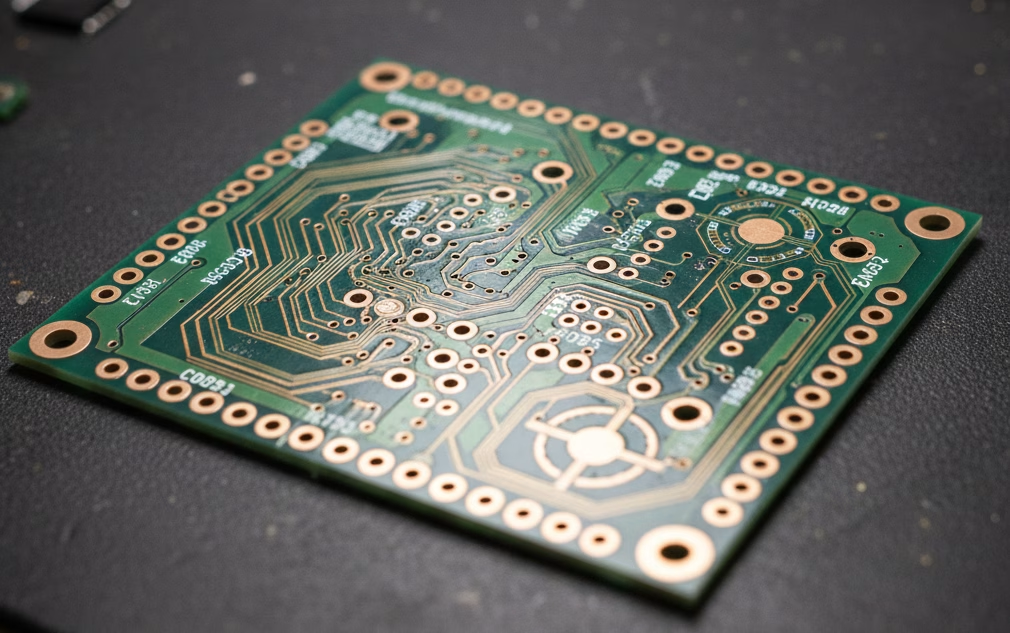
High-frequency PCBs are printed circuit boards designed to transmit signals above 1 GHz with minimal loss, distortion, or reflection. These RF circuit boards utilize low dielectric constant (Dk) and low dielectric loss (Df) laminates, such as RO4350B, RO3010, and PTFE, to maintain impedance accuracy and minimize insertion loss across GHz frequency ranges.
Precise control over dielectric thickness, copper roughness, and trace width is required to achieve consistent impedance and prevent signal degradation. Unlike standard FR4 PCBs, high-frequency designs use engineered materials with stable dielectric constants across temperature and frequency bands to minimize phase delay and signal dispersion.
High frequency PCB manufacturers make these boards for RF and microwave systems such as radar, antennas, satellite receivers, and millimeter-wave circuits, where signal integrity and consistent frequency performance are required.
Parameters To Consider For High-Frequency PCB Design:
Frequency Range: High-frequency PCBs typically operate above 1 GHz, with applications in radar systems, military equipment, aerospace, telecommunications, and high-speed digital systems.
Dielectric Constant (Dk): The dielectric constant of the PCB material affects the propagation speed of signals. Lower Dk values are preferred for high-frequency applications to minimize signal distortion and ensure accurate signal transmission.
Dissipation Factor (Df): Df represents the loss of signal energy as it travels through the PCB material. Lower Df values are desirable for high-frequency PCBs to reduce signal attenuation and maintain signal integrity.
Coefficient Of Thermal Expansion (CTE): CTE is crucial for high-frequency PCBs as it impacts the stability of the board’s dimensions under temperature variations. Low CTE materials help prevent issues like warping or delamination.
Signal Integrity: High-frequency PCB designs must minimize signal reflections, crosstalk, and electromagnetic interference (EMI) to preserve signal quality and reliability.
A High-Frequency PCB Requires the Use of Specialized Materials
Special materials are required to achieve the high frequency provided by this type of printed circuit board – any changes in the Er value of these materials can affect the impedance of the board. Many PCB designers turn to Rogers dielectric material for its lower dielectric loss, reduced signal loss, lower cost of circuit fabrication and better suitability for fast-turnaround prototyping applications.

PCBAndAssembly is an experienced full service PCB manufacturer who provides a reliable, superior-performing high-frequency PCB fabrication services.
We manufacture high-frequency PCBs with frequency typically in the range from 500MHz to 2GHz. The following table shows some of our common-use materials for High-Frequency PCBs manufacturing.
| Material | Dielectric Constant |
| RO4350B | 3.48±0.05@10 GHz |
| RO4003C | 3.38±@10 GHz |
| Ro3003 | 3.00±0.04@10 GHz |
| Ro3010 | 10.2±0.03@10 GHz |
| RT5880 | 2.20±0.02@10 GHz |
Check our capabilities by viewing the table found below:
| Feature | Capability |
| Quality Grade | Standard IPC 2 |
| Number of Layers | 2 – 24layers |
| Order Quantity | 1pc – 10000+pcs |
| Build Time | 2days – 5weeks |
| Material | RO4003C, RO4350B, Ro3003, Ro3010, RT5880 |
| PP | Rogers 4450F, Domestic-(25FR), Domestic-(RF-27), Domestic-(6700) |
| Board Size | Min 6mm x 6mm | Max 457mm x 610mm |
| Board Thickness | 0.4mm – 5.0mm |
| Copper Weight(Finished) | 0.5oz – 2.oz |
| Min Tracing/Spacing | 3mil/3mil |
| Solder Mask Sides | As per the file |
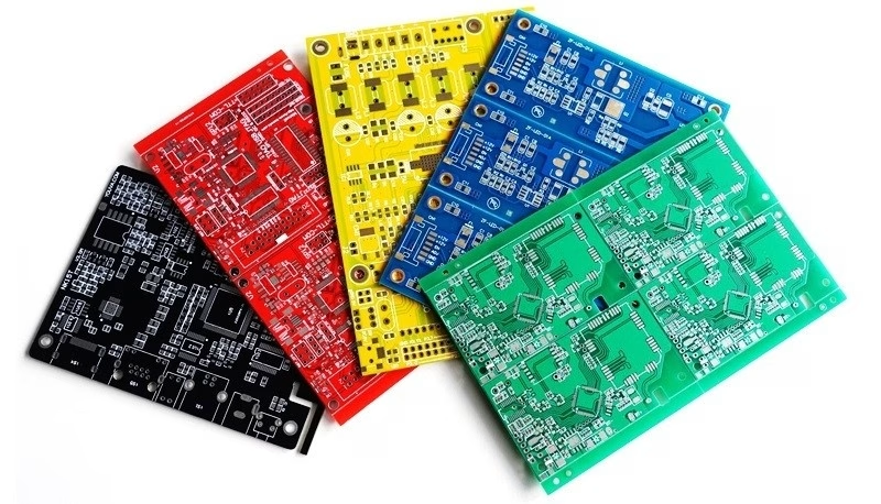
| Solder Mask Color | Green, White, Blue, Black, Red, Yellow |
| Silkscreen Sides | As per the file |
| Silkscreen Color | White, Black, Yellow |
| Surface Finish | Electroless nickel/immersion gold (ENIG) – RoHS Immersion silver – RoHS Immersion tin – RoHS Organic solderability preservatives – RoHS |
| Min Annular Ring | 4mil |
| Min Drilling Hole Diameter | 6mil |
| Impedance tolerance | ±10% |
| Other Techniques | Peelable solder mask Gold fingers Carbon oil Countersink holes |
High Frequency Material Properties
| Material | ARLON 85N | Rogers 4350B | Rogers RO3003 | Rogers RO3010 | Taconic TLX |
| Tg (°C) | 250 | 280 | — | — | — |
| CTE-z (ppm/°C) | 55 | 32 | 25 | 16 | 135 |
| Peel Strength (N/mm) | 1.2 | 0.9 | 1.2 | 1.6 | 2.1 |
| Td (°C) | 387 | 390 | 500 | 500 | — |
| Dk (@10GHz) | 4.2 | 3.5 | 3.0 | 10.0 | 2.5 |
| Loss Tangent | 0.0100 | 0.0037 | 0.0013 | 0.0022 | 0.0019 |
| Thermal Cond. (W/m·K) | 0.20 | 0.69 | 0.50 | 0.95 | 0.19 |
| Surface Resistivity (MΩ) | 1.6 × 10⁹ | 5.7 × 10⁹ | 1 × 10⁵ | 1 × 10⁵ | 1 × 10⁷ |
| Electric Strength (KV/mm) | 73 | 31 | — | — | — |
