Metal Core PCB

Contact Us

Contact us for all your PCB, PCBA, and custom service needs!

pcb

What are Metal Core PCB?

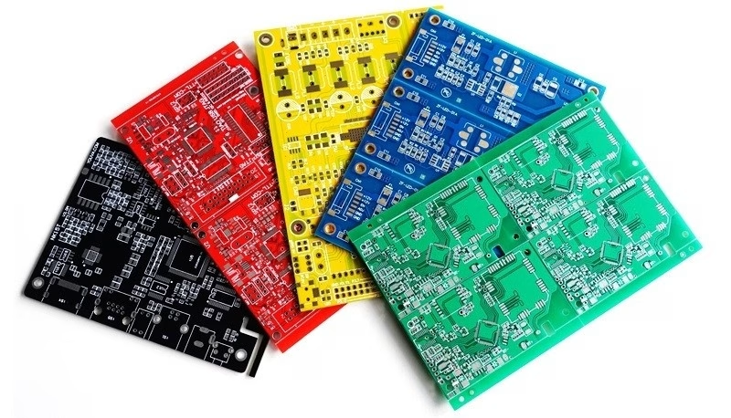
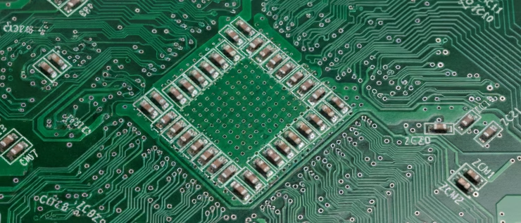
Metal Core PCBs (MCPCBs) are printed circuit boards with a metal base, typically aluminum or copper, for efficient heat dissipation. They improve thermal management, making them ideal for high-power and high-heat applications like LED lighting and power electronics. MCPCBs enhance performance and reliability by reducing heat buildup.
metal core pcb

Core Materials

We offer copper, aluminium, copper-aluminium composite, stainless steel, and iron as metal core PCB materials, each selected based on thermal conductivity, mechanical strength, and chemical compatibility.

Aluminum is used in ~85% of MCPCB builds due to its conductivity range of 1.0 to 2.2 W/m·K and low density (2.7 g/cm³), making it ideal for metal core PCB LED and general-purpose thermal designs.

Copper cores offer conductivity up to 4.0 W/m·K with higher tensile strength (210 MPa+) and are deployed in high-power PCBs, such as inverter modules and EV subsystems.

Steel and iron cores are selected where increased rigidity and resistance to deformation under load are needed, such as in vibration-exposed assemblies.

Layer Structures 

We fabricate single-layer, double-layer, and multilayer metal core PCBs using dielectric bonding and press lamination.

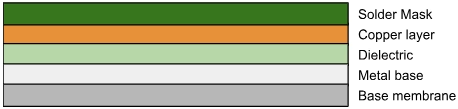
Single-sided MCPCBs consist of a copper trace layer, a thermally conductive dielectric, and a solid metal core optimized for vertical heat evacuation.

Double-sided builds use high thermal conductivity dielectric (≥2 W/m·K) on both sides of the metal substrate, allowing plated through-hole (PTH) connectivity for top/bottom side SMD assembly.

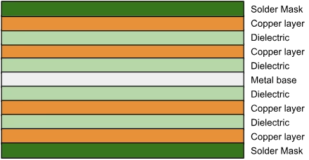
Multilayer MCPCBs use stacked copper and dielectric layers over the core, with blind/buried vias, ground/power planes, and isolation barriers, supporting high-frequency PCBs and high-density RF modules.

Thickness Range

We offer metal core thicknesses from 0.4 to 3.2mm, depending on the required mechanical rigidity and heat transfer mass.

Copper foil thickness ranges from 0.33 oz (12 μm) to 10 oz (350 μm), supporting trace widths from 0.15 mm with aspect ratios up to 10:1. Dielectric materials are applied in 50 to 125 μm layers using filled or unfilled resin systems with thermal conductivity from 1.0 to 15 W/m·K.

Minimum line/space resolution is 3 mil/3 mil with ±10% trace width tolerance after etching.

Manufacturing Process

Fabrication begins with DFM review and stack-up simulation, including thermal path modeling and expansion coefficient balancing.

Circuit imaging uses UV photoresist exposure in ISO Class 7 cleanrooms. Etching is performed with alkaline or acidic chemistries, depending on copper weight.

Mechanical or laser drilling enables via diameters down to 0.2 mm; for metal-backed PCBs, insulating collars are applied to prevent shorting.

ENIG, OSP, or HASL finishes are applied before full-panel AOI, flying probe, and impedance testing verify electrical performance.

Surface Finishing

We support industry-standard finishes including HASL (SnPb or lead-free), ENIG (Ni ≥120 μin, Au ≥2 μin), and OSP (ENTEK Plus HT).

Selective plating for high-wear pads and edge contacts is available on request. All finishes are RoHS compliant and conform to IPC-4552/4553 standards.

Surface treatments are selected based on final assembly method (e.g. reflow vs. wave soldering), component metallization, and storage duration.

Design Support

Our engineering support includes metal core and dielectric material selection, via current analysis, and thermal modeling for localized hotspot mitigation.

We review all Gerber, BOM, and stack-up files for conformity with manufacturing tolerances and suggest DFM changes such as increasing annular rings, adjusting pad clearances for aluminum etching, and evaluating heat spreading efficiency.

Design rules are calibrated to IPC-2221 standards, with optional consultation for COB MCPCB design and direct thermal path optimization.

Testing & QA

Every board undergoes 100% AOI, netlist-driven electrical testing, and visual inspection to IPC-A-610 Class 2 or 3.

For MCPCBs, we add X-ray inspection of insulated vias, microsection analysis of dielectric bond integrity, and impedance measurement on RF traces.

Boards with thermal vias are subjected to thermal shock cycling (-40 °C to +125 °C, 100 cycles) to evaluate solder joint reliability and expansion mismatch.

What Materials and Thickness Levels are used in MCPBs?

Aluminum Core PCBs

Aluminum core PCBs are the most common, offering thermal conductivity between 1.0 and 2.2 W/m·K, low density (2.7 g/cm³), and high machinability. These are widely used in LED lighting and consumer power modules where weight and cost efficiency are priorities.

Copper Core PCBs

Copper core PCBs provide thermal conductivity up to 4.0 W/m·K and higher current-carrying capacity, making them suitable for power conversion, motor control, and automotive systems. Due to its high thermal mass and reactivity, copper requires tighter etching and plating controls during fabrication.

Steel or Brass Core PCBs​

Steel or brass cores offer low thermal conductivity but high tensile strength, used primarily in assemblies requiring added structural stiffness or vibration resistance. These cores may require slower drill speeds and carbide tooling to maintain dimensional accuracy during machining.

Metal Core Thicknesses​

Metal core thicknesses range from 30 mil (0.76 mm) to 125 mil (3.18 mm), while copper foil layers are available from 1 oz (35 μm) to 10 oz (350 μm), depending on the current load and trace geometry. Thicker metal substrates may increase mechanical strength and heat-spreading mass but require specialized routing equipment and consideration of thermal expansion mismatches during lamination and soldering.

What Types of Metal Core PCBs does PCBAndAssembly Offer?

PCBAndAssembly fabricates all major metal core PCB configurations to support a wide range of thermal PCB applications. Each type is engineered to match specific thermal, electrical, and mechanical design requirements, from compact single-sided layouts to high-density multilayer stacks with advanced via structures.

Single-Sided MCPCB

This structure consists of five distinct layers: a solder mask, copper trace layer (1 to 2 oz), thermally conductive dielectric (100 to 200 μm), metal base (usually aluminum), and an optional insulating back membrane.

It offers a direct thermal path from the component side through the dielectric to the metal base, enabling rapid heat transfer. With no plated through-holes, it’s optimal for metal core PCB LED arrays, drivers, and low-complexity power circuits where components are mounted on a single side.
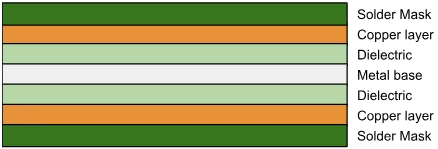
Single-Sided MCPCB

Double-Sided MCPCB

Double-sided designs feature a metal core between two copper circuit layers, separated by high thermal conductivity dielectric on each side (2.0 to 3.0 W/m·K). Through-hole plating is used for interconnects, enabling surface-mount and through-hole technology (SMT + THT).

This configuration supports denser layouts and heat spreading on both sides of the board, making it suitable for LED modules, motor controllers, and power conversion systems.

Double-Sided MCPCB

Multilayer MCPCB

Multilayer stacks integrate three or more copper layers with interleaved thermally conductive dielectric and a central or embedded metal core. The structure accommodates blind and buried vias, internal signal layers, and power/ground planes.

This architecture supports high-density interconnects and controlled impedance routing for use in automotive electronics, RF systems, and industrial high-power PCB assemblies where layered thermal management and signal integrity are required.

Multilayer MCPCB

If you’re working on projects that include Passive Infrared (PIR) Sensors, MCPCBs offer excellent thermal performance and are an ideal choice.

Project Items Our PCB Capabilities
Main Material Suppliers Shengyi, Quanbao, Xintianyuan, Juding, etc.
Metal Types Copper, Aluminum, Copper-Aluminum Composite, Stainless Steel, Iron
Structure Single-layer, Double-layer/Multilayer, Copper/Aluminum Core, Thermal-Electric Separation
Thermal-Electric Separation Flatness No significant difference(copper core boards)
Copper/Aluminum Core Thickness 0.4–3.2 mm
Copper Thickness (0.33, 0.5, 1, 2, 3, 4, 5, 6) oz, 6–10 oz requires confirmation
Insulation Layer Thickness Thermal conductive insulation: 50, 75, 100, 125, 150 μm
Others: FR4 bonding sheets
Thermal Conductivity Standard FR4, 1 W/m·K, 2 W/m·K, 3 W/m·K, up to 15 W/m·K
Max Finshed Board Size – excl. Cu Core & Thermal-Electric Separation 22.5″ × 30″
PTH Copper Base Thickness <0.8 mm: 0.8–6.0 mm
Copper Base Thickness 0.8–1.6 mm: 1.0–8.0 mm
Copper Base Thickness 1.7–3.2 mm: 1.2–8.0 mm
Countersink Holes Vertical angle: 90° ± 5°
Min drill bit: 0.8 ± 0.15 mm, Can be enlarged if needed
Depth tolerance: ±0.20 mm
Counterbore Holes Min angle: 30° ± 5°, Max angle: 180°
Min drill bit: 0.8 ± 0.15 mm, Max drill bit: 6.0 ± 0.15 mm
Depth tolerance: ±0.20 mm

How do Metal Core PCBs Compare to FR4 PCBs?

While both MCPCBs and FR4 PCBs serve as foundational substrates for electronic assemblies, their construction, thermal properties, and processing requirements differ significantly.

Metal core PCBs use a conductive metal base and thermally conductive dielectric, enabling efficient heat transfer and mechanical rigidity, whereas FR4 boards rely on woven fiberglass and epoxy resin, offering greater flexibility in thickness and design but limited thermal performance.

Aspect Metal Core PCBs FR4 PCBs
Thermal Conductivity High (1.0W to 4.0W) Low (~0.3W)
Plated Through Holes Not available for 1-layer MCPCBs Available in all PCBs
Solder Mask Only white color, typically on the top side Various colors, available on both sides
Machining Process Requires diamond-coated saw blades for V-scoring Standard machining processes
Thermal Relief Uses metal core for heat transfer, no vias required Requires vias and additional processes
Thickness Variations Limited variations Wide range of thickness options

MCPCBs are suited for high-temperature and high-power applications where managing heat buildup and maintaining stable operating conditions are important for reliable function.

Why Choose PCBAndAssembly as Your Metal Core PCB Manufacturer?

  • Metal core thickness from 0.4 to 3.2mm; copper weights from 0.33 to 10 oz.
  • Supports copper, aluminium, copper-aluminium composite, stainless steel, and iron with dielectric thermal conductivity up to 15 W/m·K.
  • Rapid prototyping and volume production with all builds 100% tested.
  • Professional Engineer Review for every project
  • Stringent Quality Control across all manufacturing processes
  • Advanced Testing Technology including AOI, E-Test, X-RAY, and Impedance Control
  • Competitive Pricing especially for multilayer Metal Core PCBs
  • ISO Certified manufacturing facilities
  • Fast Turnaround times to meet your production schedules

Metal Core PCB Manufacturer FAQs

Effective metal core PCB manufacturing starts with a well-structured design. The layer stack must define the metal core type (aluminum or copper), dielectric thickness (50 to 150 μm), and copper weight (1 to 10 oz) to balance thermal and electrical performance. For designs with plated through-holes, holes near the metal base require insulation before copper plating to prevent shorts.

Material thickness, especially in cores over 2.0 mm, affects heat spreading and increases drilling difficulty. Surface finish selection should match assembly methods and pad requirements. Designers must also account for thermal conductivity, expansion behavior, and impedance constraints tied to high-speed signals or RF paths.

Yes, plated through-holes (PTH) can be used in metal core PCBs, but only in specific structures such as double-sided or multilayer MCPCBs. In these designs, the metal core is typically located between two dielectric layers, allowing vias to pass through without contacting the conductive core.

When a via intersects the metal base, it must be insulated, either by applying a dielectric sleeve, resin fill, or via isolation layer, before copper plating. This prevents electrical shorting between the plated hole and the core. Hole diameters typically start at 0.2 mm, with positional tolerance around ±0.05 mm. Proper via clearance from the metal core (usually ≥0.3 mm) is essential to maintain electrical isolation and structural integrity.

Yes, MCPCBs can support high-frequency PCB designs, particularly when combined with low-loss dielectric materials and controlled-impedance routing.

While standard MCPCB dielectric layers have moderate Dk/Df values, hybrid builds using metal-backed RF laminates (e.g. Rogers on aluminum) enable RF performance with integrated heat dissipation. Proper stack-up planning and trace width control are essential to maintain impedance tolerance across temperature ranges.

PCBAndAssembly is certified to IATF 16949:2016, ISO 9001:2015, ISO 14001:2015, and ISO 13485:2016, reflecting our capability to support automotive, industrial, environmental, and medical applications.

All metal core PCBs are UL certified and manufactured in compliance with IPC-6012 and RoHS standards, ensuring traceability, material safety, and process consistency across every build.

Contact Us

Contact us for all your PCB, PCBA, and custom service needs!

pcb