What is Dissipation Factor (Df) in a PCB?
Dissipation Factor (Df), also known as the loss tangent (tan(δ)), is a vital parameter that measures the dielectric losses in electrical systems and components.
Get Your PCB Quote!

Table of Contents
- esittely
- Mikä on häviökerroin (Df)?
- Miten Df muuttuu signaalin vaimennukseksi
- Kemialliset perusteet: Miksi jotkut materiaalit ovat häviöllisiä
- Lasikudosilmiö: huomiotta jätetty Dk/Df-muuttuja
- Kuparin karheusrangaistus: Kun Df ei ole ainoa ongelma
- Nopean monikerroksisen pinoamisen suunnittelu
- Df:n mittaaminen ja simulointi
- FAQ
- Yhteenveto
Introduction
If you have spent years debugging 10 Gbps+ backplanes or RF front-ends, you have likely seen eye diagrams that look completely closed despite perfect impedance matching. After diagnosing hundreds of these high-speed failures , I have learned that treating the PCB substrate as a lossless insulator is the fastest way to doom a design. The culprit is almost always the Dissipation Factor (Df).
When frequencies push past 5 GHz, standard dielectric materials stop behaving like passive supports. They turn into distributed attenuators, turning your high-frequency signal energy directly into heat . Failing to account for this parameter during the initial stack-up stage leads to severe signal degradation and expensive redesign cycles.
Need PCB Manufacturing or Assembly?
Get a free quote within 24 hours. We specialize in prototype-to-production PCB/PCBA for hardware teams worldwide.
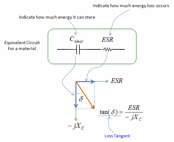
What is Dissipation Factor (Df)?
Dissipation Factor (Df), also known as the loss tangent (tan δ), represents the ratio of a dielectric material’s energy loss to its energy storage capacity under an alternating electromagnetic field. When an AC signal propagates down a PCB transmission line, the electric field polar izes the molecules of the surrounding substrate. This polarization process is not instantaneous; the molecular alignment lags behind the rapidly shifting electromagnetic field.
Mathematically, the complex permittivity of a material is expressed as:
ε = ε’ – jε”
Where ε’ is the real permittivity (which stores energy and defines the dielectric constant, Dk) and ε” is the imaginary permittivity (which represents dielectric loss). The dissipation factor is defined as the ratio of these two components:
Df = tanδ = ε” / ε’
- Energy Dissipation:The electric field forces polar molecules in the resin to physically rotate back and forth. At high frequencies, this molecular friction converts electrical power into thermal energy.
- Phase Lag:In a perfect, lossless capacitor, the current leads the voltage by exactly 9 0 degrees. In real-world dielectrics, the current leads by an angle of 90 – δ, where δ is the loss angle.
- Frequency Dependency:Df is not a static number . It varies based on the frequency of the alternating current, requiring engineers to evaluate materials at their specific target operating frequencies.
If your system operates in a high-temperature enclosure, you cannot rely on nominal 25°C Df values. At elevated temperatures, the polymer chains in epoxy resins gain mobility, allowing them to oscillate more freely under the alternating field . This increase in molecular movement directly elevates the Df of the material, requiring you to size your traces based on worst -case thermal operating conditions.
How Df Translates to Signal Attenuation
Total insertion loss in a transmission line is the sum of conductor losses (resistive skin-effect losses) and dielectric losses. While conductor loss dominates at low frequencies, dielectric loss scales linearly with frequency. Consequently, at multi-GHz speeds, the dissipation factor becomes the primary driver of signal attenuation.
The dielectric loss component of insertion loss can be calculated using the following approximation:
αd ≈ 2.3 × f × √Dk × Df
Where αd is the dielectric loss in dB per inch, f is the frequency in GHz, Dk is the dielectric constant of the laminate, and Df is the dissipation factor. This relationship demonstrates that even a slight increase in Df dramatically accelerates signal loss as frequencies climb.
| Laminate Material | Dk
(at 10 GHz) |
Df
(at 1 0 GHz) |
Loss at 1 GHz
(dB/in) |
Loss at 10 GHz
(dB/in) |
Loss at 28 GHz
(dB/in) |
| Standard FR-4 | 4 .20 | 0.0200 | 0.094 | 0.943 | 2.641 |
| Isola FR370HR | 3.92 | 0.0 150 | 0.068 | 0.683 | 1.912 |
| Panasonic Megtron 6 | 3.70 | 0.0040 | 0.017 | 0.177 | 0.495 |
| Rogers RO4350B | 3.48 | 0 .0037 | 0.015 | 0.159 | 0.445 |
| Rogers RO3003 | 3.00 | 0.0013 | 0. 005 | 0.052 | 0.145 |
This massive attenuation differential has catastrophic impacts on high-speed digital signals. When a square wave travels down a high-Df trace, its high-frequency harmonics are stripped away far faster than its fundamental frequency, rounding off the edges of the pulses. This rise-time degradation destroys the horizontal timing margin of the receiver, while amplitude attenuation eats away at the vertical noise margin.
Furthermore, because the high-frequency transitions are smeared, the electrical energy of previous bits bleeds into subsequent bits. This phenomenon, known as Inter-Symbol Interference (ISI), is the primary driver of high bit error rates (BER) in high-speed serial links. If your routing paths exceed 3 inches and your Nyquist frequency exceeds 5 GHz, choosing a material with a Df above 0.005 will likely compromise your signal integrity margins.
The Chemical Foundations: Why Some Materials are Lossy
The vast differences in Df among PCB laminates stem directly from their molecular structures. Standard FR-4 is composed of an epoxy resin matrix reinforced with woven fiberglass. The epoxy resin contains highly polar functional groups, such as hydroxyl and amine groups, which act as permanent electric dipoles. Under an alternating electromagnetic field, these polar groups rotate violently, causing high internal friction and a high dissipation factor.
To reduce this loss, material scientists must alter the polymer chemistry of the resin. By replacing highly polar epoxies with non-polar polymers, they can significantly reduce molecular rotation. Materials like polytetrafluoroethylene (PTFE), polyphenylene ether (PPE), polyphenylene oxide (PPO), and hydrocarbon resins feature highly symmetrical, non-polar molecules that experience minimal dipole moment under AC excitation.
- Non-polar Resin Backbones:Elimination of hydroxyl and other polar molecular structures prevents dipole rotation under alternating fields, dropping Df below 0.003.
- Hydrophobic Properties:Water is highly polar, with a D k of approximately 80 and a very high Df of 0.1. Materials that absorb moisture will experience rapid degradation in both Dk and Df in humid environments.
- Ceramic Fillers:Low-loss lamin ates often incorporate micro-glass or ceramic particles. These fillers help control the thermal expansion coefficient and adjust the Dk without introducing polar loss mechanisms.
When selecting a laminate for high-reliability military or aerospace hardware , remember that moisture absorption is a hidden driver of in-field Df degradation. If a board is placed in a humid environment, a standard epoxy matrix can absorb up to 0.5% of its weight in water, which will instantly destroy your tuned RF impedance and increase your channel loss.
The Glass Weave Effect: An Overlooked Dk/Df Variable
Laminates are composite materials, and their performance is not solely dictated by the resin. Woven glass fabrics have a high Dk (~6.1) and extremely low Df (~0.003), while the surrounding resin typically has a lower Dk (~3.0) and higher Df (~0.02). This mismatch in material properties creates localized dielectric boundaries throughout the board.
When a differential trace runs over a standard open-weave glass fabric (such as 1060 or 1080), one leg of the differential pair may run directly over a glass bundle (glass-rich area), while the other leg runs over a gap filled with pure resin (resin-rich area). Because of this misalignment, the two signals experience different propagation velocities and unequal attenuation rates, leading to skew and phase distortion.
| Glass Weave Style | Yarn Count
(Warp x Fill) |
Open Area
(%) |
Typical Thickness
(mil) |
Skew Risk |
| 106 | 56 x 56 | 12% | 1.3 | High |
| 1 080 | 60 x 47 | 8% | 2 .5 | High |
| 1078 | 54 x 54 | 1% | 1.7 | Low |
| 3313 | 44 x 4 4 | <1% | 3.3 | Very Low |
To eliminate this skew and loss variation, you should specify spread-glass weaves (such as 1078 or 3313) in your fabrication notes. Mechanically spread -glass weaves feature tightly flattened glass bundles that close the gaps between fibers. This flat, uniform profile minimizes localized variations in both dielectric constant and dissipation factor across the board.
If you cannot use spread-glass weaves due to cost or lead-time constraints, you can mitigate the glass-weave skew by routing your high-speed differential pairs at a 10 to 45-degree angle relative to the weave grid. This technique averages out the exposure of both traces to the glass and resin bundles, ensuring that both signals see a uniform average dielectric constant and dissipation factor.
The Copper Roughness Penalty: When Df Is Not the Only Problem
At high frequencies, current does not flow through the entire cross-section of a trace. Due to the skin effect, current is forced to flow along the outer perimeter of the conductor. The skin depth at 10 GHz is approximately 0 .66 microns. If the surface of the copper foil is rough, the high-frequency current must travel along the physical contours of the rough interface.
This extended path length increases the effective resistance of the conductor, resulting in significant resistive loss. Furthermore, the tooth-like structures of rough copper project directly into the surrounding prepreg, creating a capacitive interface that stores additional energy in the lossy dielectric. This interaction artificially inflates the measured “effective” Df of your transmission line, making even a high-quality, low-loss laminate behave poorly.
| Copper Foil Type | Roughness
(Rz, µm) |
Relative Loss at 20 GHz | Primary Application |
| ED (Standard Electrodeposited) | 6.0 – 10.0 | 100% ( Baseline) | Low-frequency power and control signals |
| V LP (Very Low Profile) | 2.0 – 3.0 | 65 % | High-speed digital up to 10 Gbps |
| HVLP (Hyper Very Low Profile) | 0.8 – 1.5 | 45% | 28 Gbps+ SerDes and RF up to 40 GHz |
| RA (Rolled Annealed) | < 0.5 | 30% | Flexible circuits and high-precision mmWave RF |
I’ve seen boards come back with 12 dB of unexpected attenuation at 12. 5 GHz because the fabrication house substituted a generic mid-loss prepreg for the Megtron 6 I specified. When we analyzed the cross-section under a scanning electron microscope, we discovered they had also used standard electrodeposited (ED) copper on the inner signal layers. The combined effect of the incorrect laminate and rough copper completely closed the receiver’s eye diagram, rendering the prototype assembly useless.
To avoid this failure mode, always ensure that your high-speed laminates are specified with Very Low Profile (VLP) or Hyper Very Low Profile (HVLP) copper. For frequencies above 20 GHz , standard ED copper is unusable because its average surface roughness is several times larger than the skin depth, completely wiping out any loss benefits of your expensive low-loss dielectric.
About PCBAndAssembly
Time is money in your projects – and PCBAndAssembly gets it. PCBAndAssembly is a PCB assembly company that delivers fast, flawless results every time. Our comprehensive PCB assembly services include expert engineering support at every step, ensuring top quality in every board. As a leading PCB assembly manufacturer, we provide a one-stop solution that streamlines your supply chain. Partner with our advanced PCB prototype factory for quick turnarounds and superior results you can trust.
Designing a High-Speed Multilayer Stack-up
When designing a complex, multi-layer board, specifying low-loss materials across the entire stack-up is rarely a viable financial option. A 16-layer board built entirely out of high-frequency PTFE lamin ates is highly expensive and difficult to manufacture due to material registration issues. Instead, you should utilize a hybrid stack-up design.
A hybrid stack-up combines high-frequency, low-loss prepreg and core materials on the critical outer layers with cheaper, high-reliability FR-4 cores in the center of the board. This approach allows you to route critical high-speed differential pairs and RF traces on the high-performance layers while routing low-speed control lines and power distribution networks through the low-cost FR-4 core layers.
| Layer | Material | Thickness
(mils) |
Function | Dk/Df Requirement |
| L 1 (Top Signal) | Megtron 6 Prepreg | 4.0 | High-Speed RF and Differential Pairs | Dk 3.7 / Df 0.004 |
| L2 (Ground) | HVLP Copper Foil | 1.2 | Reference Plane | N/A |
| L3 (Power/Signal) | Standard FR-4 Core | 12.0 | Low-speed digital routing and power planes | Dk 4.2 / Df 0.020 |
| L4 (Power) | Standard FR-4 Core | 12.0 | Power Distribution Network (PDN) | Dk 4.2 / Df 0.0 20 |
| L5 (Ground) | HVLP Copper Foil | 1.2 | Reference Plane | N/A |
| L6 (Bottom Signal) | Megtron 6 Prepreg | 4.0 | High-Speed RF and Differential Pairs | Dk 3.7 / Df 0.004 |
When executing a hybrid design, it is critical to balance the thermal expansion coefficients (CTE) of the dissimilar materials. Low -loss PTFE materials tend to expand much faster in the Z-axis than standard FR-4 epoxies. If the thermal profiles are not balanced during lamination, the board will warp, and the internal copper plating of your through-hole vias may tear away from the internal pads during lead-free reflow.
To prevent these mechanical failures, work with your fabrication house to ensure that the lamination temperature profiles and cure times are compatible for all selected materials. Always place your high-frequency layers symmetrically about the center of the vertical stack-up to prevent unbalanced stress distributions during thermal cycling.
How to Measure and Simulate Df
Laminate manufacturers measure material properties under ideal lab conditions that do not match the geometric realities of your actual PCB layout. Standard datasheets typically report Df values measured using the Clamped Stripline method (IPC-TM-650 2.5.5.5) or the Split Post Dielectric Resonator (SPDR) method. These tests use flat, unclad dielectric samples, ignoring the impacts of copper roughness, via transitions, and weave skew.
To obtain a realistic estimate of system performance, you must use frequency -dependent material models in your EDA software. Standard simulators that assume a static, non-varying Df will underestimate your actual high -frequency losses, yielding overly optimistic simulation results that fail to match bench-top measurements.
- Use Frequency-Dependent Models:Utilize models such as the Svensson-Djordjevic or wideband Debye models in your simulation tools (e.g., Ansys HFSS or Cadence Sigrity) to capture how Dk and Df shift with frequency .
- Incorporate Copper Roughness Models:Apply the Hammerstad-Beketenev or Huray roughness models in your simulator, using the actual Rz roughness value of your specified copper foil to predict resistive losses.
- Verify on the Bench:Fabricate a test coupon featuring a multi-inch microstrip and stripline path. Use a Vector Network Analyzer (VNA) or Time Domain Reflectometry (TDR) to measure the actual insertion loss, matching the measured data back to your simulation models.
Always request the material supplier’s multi-frequency data curves rather than relying on the single-frequency values on the first page of the datasheet. A material that boasts a highly attractive Df of 0.002 at 1 GHz may exhibit a significantly higher Df at your target operating frequency of 2 8 GHz.
FAQ
Does Df affect the characteristic impedance of a trace?
No, characteristic impedance is primarily driven by trace geometry and the real part of the permittivity (Dk). Df directly controls signal attenuation and losses, but it has a negligible effect on the physical impedance of the trace.
Why does a higher Df generate more heat in a PCB?
When high-frequency AC signals pass through a lossy dielectric, the polar molecules in the resin rotate rapidly. This friction converts a portion of the electromagnetic signal energy into thermal energy, raising the operating temperature of the board.
Can I use standard FR-4 for 5 GHz signals if the routing distances are very short?
Yes. If your trace lengths are under 1 to 2 inches, standard FR-4 may be acceptable since the total accumulated loss is proportional to the physical path length. However, you must simulate the path to verify that the signal margins remain acceptable.
How does water absorption impact a material’s Df?
Water is highly polar, possessing a very high dissipation factor of 0.1. Consequently, even minor moisture absorption in humid environments will significantly elevate the effective Df of a laminate, causing unexpected signal attenuation and impedance shifts.
Summary
Understanding and managing Dissipation Factor (Df) is crucial when designing high-speed digital and RF circuits. While standard materials like FR-4 are sufficient for lower frequencies, their high polar molecule content turns them into lossy attenuators at speeds above 5 GHz. By transitioning to low-loss, non-polar resin systems, specifying flattened glass weaves, and selecting low-profile copper foils, you can preserve signal integrity and minimize thermal dissipation.
My final piece of advice: do not rely solely on the first-page datasheet values. Request the frequency-versus-Df curves from your laminate supplier at your specific resin content, and design your channels with at least a 20% loss margin to account for manufacturing tolerances and copper roughness.

Get Quote Free