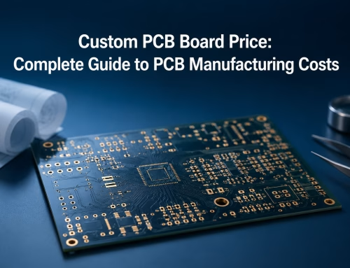
Ball Grid Array Rework Demystified
This article will introduce how to use correctly the ball grid array rework station for BGA repair, helping you better master this technology. At PCBAndAssembly, we specialise in professional PCBA services, utilizing advanced soldering techniques and X-ray inspection for both BGA, surface-mount, and through-hole components
Get Your PCB Quote!

Table of Contents
BGA (Ball Grid Array) has become a widely used packaging form in modern electronic devices. BGA rework refers to removing a BGA device from a PCB and then re-soldering it to the PCB when it fails.
But it’s hard to observe solder joints. Reworking BGAs is complex, so the BGA chip rework is still a challenge for some unskilled repair personnel. Fortunately, the BGA rework station can solve this problem. This article will introduce how to use correctly the BGA rework station for BGA repair, helping you better master this technology.
What Does BGA Meaning?
A BGA (Ball Grid Array) chip is integrated circuit packaging. Solder joints on the bottom of the chip are in circular or cylindrical arrays. The solder balls connect to the PCB pads through a reflow soldering process.
BGA packaging has many advantages, such as small size, high density, and good heat dissipation performance, and is widespread in consumer electronics, communication equipment, industrial control, and other fields.
According to the type of BGA packaging material, BGA components can be divided into:
- Plastic Ball Grid Array (PBGA) — most common, cost-effective, used in consumer electronics
- Ceramic Ball Grid Array (CBGA) — high reliability, used in aerospace and military
- Ceramic Column Grid Array (CCGA) — columns instead of balls, better thermal cycling
- Tape Ball Grid Array (TBGA) — thin and flexible, used in space-constrained designs

What Are the Reasons for BGA Rework?
1)Device Fault
Failure in Ball Grid Array connections can cause a device to stop working or performance degradation.
2)Temperature Issues
The stability of BGA connections is affected by temperature changes. If the temperature is too high or too low, it may lead to the solder falling off or deforming.
3)Stress Issues
Due to mechanical stress and vibration, etc., stress may occur in the BGA connection, causing the solder to break.

4)Production and Design Defects
During the manufacturing process, there may be problems with the location and layout of BGA components, resulting in poor connections.
5)Maintenance and Repair
During maintenance or repair, incorrect operation or use of inappropriate tools may damage the Ball Grid Array connection.
Advantages of BGA Rework
Low rework cost: reworking a BGA chip is cheaper than replacing the entire circuit board.
• Fast Repair
It usually takes less time than remanufacturing the PCB and replacing surface mount components.
• Reliability Improvement
Through rework, problematic BGA connections can be repaired, improving the reliability and performance of the device.
• Environmental Protection
Through repair, We can reduce electronic equipment waste. It will also lessen the burden of electronic garbage on the environment.
How to Choose a BGA Rework Station
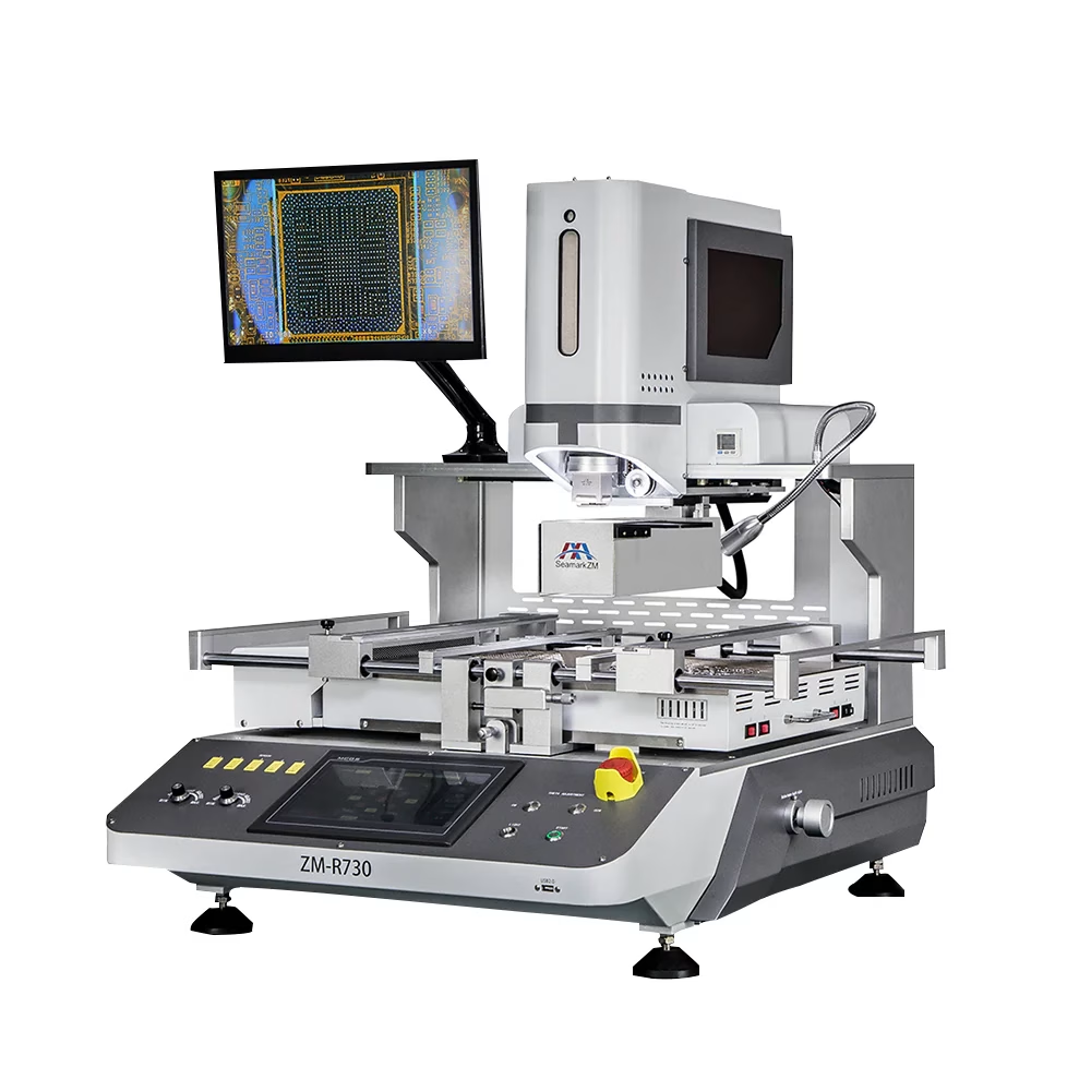
Choosing the right BGA rework station is critical for achieving consistent, high-quality results. Here are the key factors to consider:
Key Technical Parameters
- Upper heater power: typically 800W–1500W for hot air nozzle heating
- Lower heater power: typically 600W–1200W for PCB preheating
- Temperature accuracy: ±2°C or better for reliable reflow control
- Optical alignment system: prism or camera-based vision alignment for precise chip placement
Station Types
Split-type stations separate the upper and lower heating units, offering more flexibility for large PCBs. Integrated stations combine everything in one unit, ideal for small-shop or mobile repair environments.
Choosing by Application
| Application | Recommended Type | Key Feature |
| Smartphone repair | Integrated, compact | Optical alignment, fine temperature control |
| Industrial / server PCB | Split-type, high power | Large nozzle support, bottom preheating |
| R&D / prototyping | Programmable | Flexible curve programming, data logging |
Understanding the Reflow Temperature Profile
The reflow temperature profile is the most critical parameter in BGA rework. An incorrect profile is the leading cause of defects such as bridging, head-in-pillow, and chip warpage. A standard profile consists of four stages:
Stage 1 — Preheat
The PCB and chip are gradually brought up from room temperature to around 150°C. The recommended ramp rate is 1–3°C per second. Too fast a ramp causes thermal shock; too slow wastes time and risks oxidation.
Stage 2 — Soak (Thermal Equalization)
Temperature is held between 150°C and 180°C for 60–120 seconds. This allows the entire board to reach a uniform temperature and activates the flux, removing oxides from the solder surfaces.
Stage 3 — Reflow
Temperature rises above the solder melting point. For lead-free solder (SAC305), the peak temperature is typically 240–250°C. For leaded solder (63/37 Sn-Pb), the peak is around 210–220°C. Time above liquidus (TAL) should be kept to 30–60 seconds.
Stage 4 — Cooling
The board cools at a controlled rate, ideally 2–4°C per second. Rapid cooling can cause thermal stress and micro-cracks in solder joints. Natural cooling is too slow and may cause grain coarsening.
Ball Planting Process in Detail
Ball planting (reballing) is one of the most skill-intensive steps in BGA rework. Properly replanted solder balls are essential for a reliable connection.
Method 1 — Stencil Method (Recommended)
A laser-cut stainless steel stencil with holes matching the BGA pad layout is placed over the chip. Solder balls are poured across the stencil and settle into each hole. This method delivers consistent ball placement and is the preferred approach for production environments.
Method 2 — Manual Placement
Individual solder balls are placed by hand or with a vacuum pen. This method is slower and more prone to error but is suitable when no stencil is available.
Solder Ball Selection
- Ball diameter must match the original specification (commonly 0.3mm, 0.4mm, 0.5mm, 0.76mm)
- Use SAC305 (Sn96.5/Ag3/Cu0.5) balls for lead-free designs; Sn63/Pb37 for leaded designs
- Apply a thin layer of reballing flux before placing balls to hold them in position during reflow
Common Ball Planting Defects
- Missing balls: caused by insufficient flux or stencil misalignment
- Ball displacement: caused by vibration during placement or insufficient flux
- Ball bridging: caused by solder balls that are too large or stencil openings that are too close
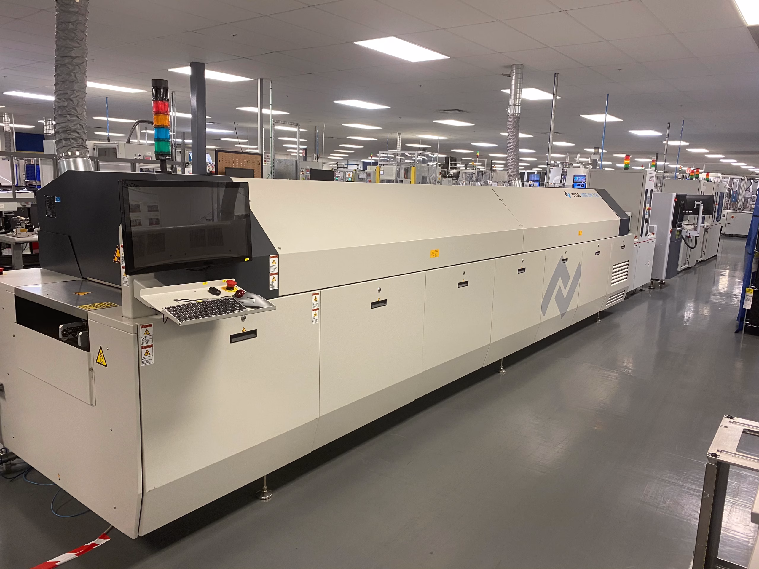
BGA Rework Flow

BGA repair is a complex process that requires strict compliance with the corresponding processes and operating specifications to ensure soldering quality. Now, Now, technicians use BGA rework stations for repairs. Because it includes tools such as hot air guns, hot plates, microscopes, etc, it can help maintenance personnel accurately control the temperature and soldering process.
The BGA rework process mainly includes the following steps:
1) Preparation
Drying: Dry the circuit boards and chips to remove moisture. It prevents product defects during the rework, such as bubbles or open circuits.
Product protection: Protect components on circuit boards susceptible to heat damage, such as plastic parts, LEDs, batteries, etc.
Preparation of nozzles and supports: Choose the suitable nozzles and supports. Do this based on the size and thickness of the circuit board. It will prevent the board from deforming.
Disassembly or soldering curve: Pick the right disassembly or soldering curve. Do this based on the type and spec of the chip. It prevents damage to the chip or board.
2) Disassembly
Select the appropriate temperature curve and remove the BGA device from the circuit board.
Cleaning solder pads: Remove residual solder paste and solder balls on the PCB.
3) Ball Planting
Select appropriate solder balls and auxiliary materials, and implant the solder balls onto the pads of the BGA parts.
4) BGA Soldering
Choose appropriate auxiliary materials ( tin or flux paste ) and apply them evenly on the pad.
Solder the BGA device to the circuit board.
After the surface mount inspection, choose the temperature curve for the chip. Heat the BGA with it. Then, remove the PCB after it cools.
5) Detection
Use X-ray detection to check for defects such as cold welding, open circuits, short circuits, etc. It ensures the welding quality is qualified.

X-Ray Inspection for BGA Quality Verification
Because BGA solder joints are hidden beneath the chip, visual inspection is impossible. X-ray inspection is the only reliable method to verify joint quality without destructive testing.
What to Look for in X-Ray Images
- Voiding: Gas pockets trapped inside solder joints appear as dark circles. IPC-7095D allows a maximum void area of 25% per joint for most applications.
- Bridging: Two adjacent pads connected by solder, causing a short circuit.
- Open circuit: A missing or collapsed solder ball with no connection.
- Head-in-Pillow (HIP): The ball and the pad solder don’t fully coalesce — appears as a shadow or dimple within the ball in the X-ray image.
- Misalignment: The ball pattern is shifted relative to the pad pattern.
2D vs. 3D CT X-Ray
Standard 2D X-ray provides a flat projection view, suitable for detecting bridging, opens, and gross voiding. 3D CT (Computed Tomography) X-ray reconstructs a three-dimensional image of each joint, allowing precise void volume measurement and detection of subtle HIP defects. 3D CT is the gold standard for critical or high-reliability applications.
Common BGA Rework Defects and Solutions
| Defect | Primary Cause | Solution |
| Chip warping | Overheating or uneven heating | Control ramp rate; increase bottom preheat |
| PCB warping | Excessive top heat, poor support | Lower top temp; adjust board support height |
| Head-in-Pillow (HIP) | Chip warpage + insufficient reflow | Improve coplanarity; extend time above liquidus |
| Solder voiding | Flux outgassing, insufficient preheat | Extend soak stage; use low-void flux |
| Bridging | Excess solder / flux, stencil issues | Check stencil aperture; reduce flux volume |
| Open circuit | Poor coplanarity or low peak temp | Verify ball height; re-check temperature curve |
| Cold joint | Insufficient peak temperature or TAL | Increase peak temp or extend TAL slightly |
Common Issues in BGA Rework
Chip warping: Control the temperature and time during disassembly, pad cleaning, and ball planting to prevent the chip from overheating and deformation.
PCB warping: Lower the temperature and increase the bottom heating temperature. Also, watch the support position and height to prevent PCB deformation.

Welding open circuit: Check welding curve, auxiliary materials, drying, and coplanarity to ensure welding quality.
Welding short circuit: Check the stencil opening, drying, solder mask, and temperature curve to prevent welding short circuits.
BGA Rework Notes
• Strictly follow the repair process and operating specifications to prevent repair failure.
• Use appropriate equipment and materials to ensure welding quality.
• Be familiar with common problems in BGA chip rework and prepare countermeasures.
BGA Rework FAQ
Question 1: What is the main challenge of BGA rework compared to other surface-mount components?
Answer: The primary challenge is that the solder balls and joints are hidden underneath the component, making visual inspection and direct soldering impossible. This necessitates specialized equipment like BGA rework stations with vision systems and controlled heating.
Question 2: Can I use a standard hot air gun for BGA rework?
Answer: While a standard hot air gun might be used for very simple, non-critical BGAs or for component removal, it lacks the precise temperature control, bottom heating, and optical alignment necessary for reliable, high-quality BGA rework. It significantly increases the risk of damage to the component or PCB .
Question 3: What is “reballing” in BGA rework?
Answer: Reballing is the process of applying new solder balls to a BGA component, typically done when reusing a component that was removed from a board, or when changing the solder alloy type. It involves applying flux, positioning a stencil, placing new solder balls, and then reflowing them onto the component pads.
Question 4: How important is thermal profiling?
Answer: Thermal profiling is critically important. It ensures that the component and PCB are heated and cooled at controlled rates to prevent thermal shock, board warping, and component damage, while also achieving proper solder reflow. Incorrect profiling is a leading cause of rework failures.
Question 5: What are common signs of a failed BGA rework?
Answer: Common signs include the device still not functioning, intermittent failures, visible solder bridges or opens under magnification (if inspectable), lifted pads, board warping, or signs of overheating like charring or discoloration. X-ray inspection is the most reliable method for detecting hidden defects.
Summary
BGA repair is a complex process that requires skill and experience. Although BGA technology is more advanced, chip performance will decrease under multiple stress impacts. Therefore, PCBA manufacturers should strengthen supervision and management when packaging chips to minimize the probability of BGA rework.
Mastering the full rework workflow — from choosing the right rework station and understanding reflow temperature profiles, to precise ball planting, correct soldering, and thorough X-ray inspection — is essential for achieving consistently reliable results. As BGA packages continue to shrink and ball counts increase, investing in proper equipment and training becomes more important than ever.

Get Quote Free