SMT vs. Through- Hole Components: Engineering Guide
Discover the critical mechanical, electrical, and thermal differences between SMT and through-hole components to optimize your next PCB layout.
Get Your PCB Quote!
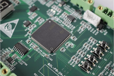
Table of Contents
- Bevezetés
- Mechanikai integritás és összekapcsolási szilárdság
- Elektromos paraziták és nagyfrekvenciás teljesítmény
- Hőgazdálkodás és hőelvezetés
- Összeszerelési munkafolyamatok és gyártóberendezések
- Csomagbesorolások és szabványok
- Gyártásra tervezés (DFM) és hibamódok
- Teljes tulajdonlási költség (TCO) és beszerzés
- FAQ
- Összegzésként
Introduction
Modern printed circuit board (PCB) design requires a clear understanding of the mechanical, electrical, and thermal differences between Surface Mount Technology (SMT) and Through-Hole Technology (THT).
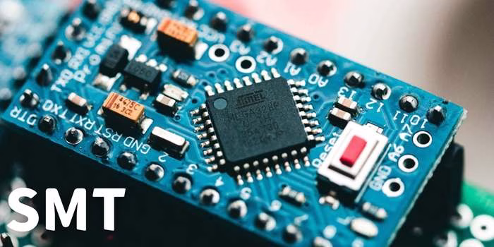
SMT involves mounting Surface Mount Devices (SMDs) directly onto the copper pads of a board’s surface.
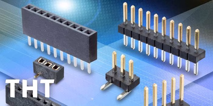
In contrast, Through-Hole Technology requires component leads to be inserted into plated-through holes (PTH) drilled through the PCB substrate, with the leads soldered to pads on the opposite side or within the barrel of the hole.
The choice between these two methodologies is rarely an all-or-nothing decision. Modern complex boards are frequently mixed-technology assemblies, combining SMT for high-density processors, memory, and passives, with THT for connectors, power semiconductor packages, and heavy inductive components. Selecting the incorrect mounting style can lead to field failures under mechanical stress, signal integrity degradation in high-speed lines , or unnecessary assembly costs during mass production.
Mechanical Integrity and Interconnect Strength
Mechanical stress is a primary failure vector for solder joints. The structural differences between SMT and THT interconnects determine their resistance to various physical forces, including shear, tension, vibration, and thermal cycling.
THT components derive their mechanical robust strength from the physical insertion of the copper lead through the FR4 glass-epoxy laminate. When the lead is soldered, a continuous solder cylinder fills the plated-through hole, wetting both the component side pad, the inner barrel, and the solder side pad. This structure distributes mechanical loads through the Z-axis of the entire board substrate rather than concentrating the stress at the copper-laminate interface.
Conversely, SMT components rely solely on the adhesion of the copper land pad to the PCB laminate, along with the shear strength of the surface solder fillet. The adhesion strength of a standard FR 4 copper pad is limited, with peel strengths typically around 1.1 to 1.4 N/mm ( 6 to 8 lb/in) for 1 oz copper. Heavy SMT components subjected to high shock, sustained vibration, or connector mating forces can easily shear the pad directly off the fiberglass substrate. Consequently, components subjected to external physical forces—such as RJ 45 jacks, USB-C ports, terminal blocks, and heavy electrolytic capacitors—remain predominantly THT in industrial, automotive, and aerospace applications.
| Mechanical Parameter | Surface Mount Technology (SMT) | Through-Hole Technology (THT) |
| Primary Load-Bearing Element | Surface solder fillet and copper-laminate bond | Physical copper lead inside plated -through hole (PTH) barrel |
| Vibration and Shock Resistance | Moderate to poor for heavy/tall components; excellent for low-mass passives | Excellent; physically anchored through the substrate |
| Typical Failure Mode | Pad cratering, solder joint shear , or component cracking | Lead fatigue, solder joint cracking at the copper-pin boundary |
Electrical Parasitics and High-Frequency Performance
The electrical geometries of SMT and THT packages diverge significantly, directly impacting signal integrity, electromagnetic compatibility (EMC), and high-frequency operational limits.
T HT components exhibit substantial parasitic inductance and capacitance due to their long physical leads and the copper barrels of the plated-through holes. A standard component lead of 0.8 mm diameter exhibits approximately 1 nH of parasitic inductance per millimeter of length. When combined with the capacitive coupling between the PTH barrel and internal reference planes (typically 0.5 pF to 2 p F depending on board stackup and clearance trace geometries), THT structures act as low-pass filters or parasitic resonators. At signal frequencies above 100 MHz, or on digital signal edges with sub-nanosecond rise times, these parasitics cause signal reflections, ground bounce, and electromagnetic radiation (EMI).
SMT packages minimize or eliminate leads entirely. For example, Ball Grid Array (BGA) and Quad Flat No-Lead (QFN) packages utilize solder balls or flat landing pads, reducing loop inductance to less than 0.5 nH and parasitic capacitance to negligible levels. Shorter interconnect paths translate directly to reduced loop areas, which minimizes radiative emissions and susceptibility to external electromagnetic fields. For high-speed digital interfaces (such as PCIe , DDR, and high-frequency RF networks), SMT is mandatory.
Thermal Management and Heat Dissipation
Thermal dissipation pathways differ fundamentally between surface mount and through-hole configurations. Power electronics designers must calculate these thermal impedances when selecting component packages for high-current applications.
THT power packages, such as the TO-220, TO-247, or TO-3, are designed to dissipate heat primarily into external metal heatsinks. Because the package stands vertically or is bolted directly to a chassis, the bulk of the thermal energy bypasses the PCB substrate. This keeps the glass transition temperature (Tg) of the FR4 laminate (typically 130°C to 170°C) from being exceeded during operation. The thick copper leads of THT packages also provide a low-thermal-resistance path directly into the internal ground and power planes of the board.
SMT power packages, such as D2PAK (TO-263) or power QFNs with exposed thermal pads, rely on the PCB itself as the primary heatsink. Heat must be conducted from the silicon junction, through the package’s thermal pad, and into the surface copper pour. To transfer this heat to internal or bottom-layer copper planes, designers must place arrays of thermal vias directly beneath the component pad. If these vias are not properly designed—typically 0.3 mm diameter with 1 oz copper plating inside the barrel —the thermal resistance (RθJA) will spike, leading to thermal runaway and component failure.
| Thermal Property | SMT (e.g., D2PAK / Power QFN) | THT (e.g., TO-220 / TO-247) |
| Primary Thermal Path | Conduction through PCB surface copper and internal thermal vias | Con duction through leads and direct convection/conduction to external heatsinks |
| Typical Thermal Impedance (RθJA) | 0.5°C/W to 3°C /W (highly dependent on PCB layout) | 0.4°C/W to 1.5°C/ W (independent of PCB layout) |
| Required PCB Real Estate for Cooling | Large copper pours and thermal via arrays are mandatory | Minimal on-board area; relies on vertical volume and heatsink brackets |
Assembly Workflows and Manufacturing Equipment
The choice between SMT and THT dictates the assembly equipment line, process flow, and manufacturing throughput. High-volume electronic assembly relies almost exclusively on the high -speed automation of SMT lines.
The SMT Process Flow
The SMT assembly process is linear, highly repeatable, and fully automated:
- Solder Paste Printing :A metal stencil deposits lead-free solder paste (typically SAC305) onto the PCB land pads with sque egee blades.
- Automated Pick-and-Place:SMT pick-and-place machines extract components from tape-and-reel feeders and position them onto the paste at rates exceeding 100,000 components per hour (CPH) with micron-level precision.
- Reflow Soldering:The board passes through a multi-zone reflow oven. The temperature profile carefully ramps up to melt the solder alloy, wet the terminals , and cool to form solid, intermetallic joints.
The THT Process Flow
Through-hole assembly is more mechanically complex and requires specialized processing stages:
Lead Prep and Insertion: Leads must often be cut, bent, and formed before insertion. This insertion can be executed via automated axial/radial insertion machines or manual labor for odd-form components.
Wave Soldering: The stuffed PCB is fluxed, preheated, and passed over a wave of molten solder. The solder wicks up into the plated-through holes by capillary action.
Selective Soldering: On mixed-technology boards where wave soldering would destroy pre-applied SMT components on the bottom side, a selective soldering machine uses a small, programmable nozzle of molten solder to target individual THT pins.
Package Classifications and Standards
Component geometries are standardized by organizations such as JEDEC and IPC to ensure compatibility across manufacturers and pick-and-place systems . Understanding these standard packages is essential for footprint creation and layout design.
SMT Package Types
- Passive Chip Packages:Metric and Imperial designations define the length and width of resistors and capacitors (e.g ., 0402 Imperial is 1.0 mm x 0.5 mm; 0201 Imperial is 0 .6 mm x 0.3 mm).
- Small Outline Packages:SOP, SOIC, and SOT packages feature gull-wing leads extending outward from the silicon package, offering accessible probe points and reliable solder fillets.
- Grid Arrays and Bottom-Termination Components:BGA, QFN, and Land Grid Array (LGA) packages place connections underneath the body of the device. This maximizes pin density but requires Automated X-Ray Inspection (AX I) to verify joint integrity.
THT Package Types
- Ax ial Leaded:Leads exit from opposite ends of a cylindrical component (commonly used for low-power resistors and diodes) and lie flat against the board during horizontal mounting.
- Radial Leaded:Leads exit from one side of the component (typically used for ceramic disk capacitors, transistors, and electrolytic capacitors), saving board area by standing vertically .
- Dual In-line Packages (DIP):Two parallel rows of pins designed to fit standard 0.1-inch (2.54 mm) grid spacing, commonly used for legacy integrated circuits, optocouplers, and DIP switches.
| Package Class | Examples | Pitch (Typical) | Main Application |
| SMT Passive | 0201, 0402, 0603, 1206 | N/A (Two-terminal) | Decoupling, filtering, impedance matching |
| SMT Leadless | QFN, DFN, LGA | 0. 4 mm to 0.65 mm | Microcontrollers, power management ICs, sensors |
| SMT Array | BGA, Flip-Chip | 0 .5 mm to 1.27 mm | High-pin-count processors, FPGAs, SoC devices |
| THT Discrete | TO-220, TO-9 2, DO-41 | 2.54 mm | Power transistors, rectifiers, voltage regulators |
| THT Multi-pin | DIP8, DIP1 6, Pin Headers | 2.54 mm | Connectors, legacy logic ICs, user-service able parts |
Design-for-Manufacturing (DFM) and Defect Modes
Both technology classes are subject to assembly defects if design rules are not strictly aligned with IPC-735 1 (for SMT footprints) and IPC-2221/2222 (for THT design).
SMT Defect Mechanisms
- Tombstoning:This occurs during reflow when one pad of a two-terminal component (like an 0402 resistor) reaches liquid us temperature before the other. The surface tension of the molten solder pulls the component upright, breaking the electrical connection on the cold side. Balanced thermal routing and symmetrical pad traces prevent this.
- Solder Bridging:Fine -pitch SMT components (such as 0.4 mm pitch QFPs) are prone to solder bridging if paste volume is excessive or pad placement is too close. High-accuracy stencil design and proper solder mask dams between pads mitigate this risk.
- Voiding:Voids occur under large thermal pads and BGA balls when trapped flux volatiles cannot escape during reflow. Voiding can be reduced by partitioning large thermal pads into arrays of smaller pads and applying a cross-hatch solder paste pattern.
THT Defect Mechanisms
- S older Starvation (Incomplete Fill):IPC-A-610 Class 3 standards require a minimum of 75% vertical solder fill inside the plated-through hole barrel. Solder starvation occurs if the thermal relief on power planes is insufficient, causing the copper planes to act as heat sinks that freeze the solder before it can flow to the top of the board .
- Outgassing and Pinholes:Moisture trapped inside the FR4 epoxy matrix can evaporate during wave soldering. This steam escapes through the copper barrel plating, creating voids, pinholes, or blowholes in the solidifying solder joint. Baking boards before assembly removes this moisture.
- Solder Webbings and Icicles:Excess dwell time in wave soldering or degraded flux activity can cause molten solder to form sharp points (icicles) or fine bridges across adjacent leads. Proper lead protrusion lengths (typically 1.5 mm to 2.0 mm) and correct wave transport speeds prevent these defects.
Total Cost of Ownership (TCO) and Procurement
When selecting components, procurement managers and design engineers must calculate the total cost of ownership, which goes beyond the line-item component cost listed on a Bill of Materials ( BOM).
At low production volumes, such as prototype runs of 1 to 100 boards, THT can be highly cost-effective because it allows for hand assembly without expensive tooling. No stencils, pick -and-place files, or complex reflow profiling thermal setups are required. Technicians can solder components using standard workbench tools.
At medium to high production volumes, the economics shift completely. THT is slow and labor-intensive. Even when using wave or selective soldering machines, manual placement of odd-form THT components is often necessary, which increases labor costs and cycle times. Additionally, THT boards require drilled holes, which increases raw PCB fabrication costs because drill bit wear and registration processing add to the manufacturer’s overhead.
SMT components are optimized for high-volume automation. The components are packed in tape-and-reel format, which is inexpensive to ship and store . Because SMT allows components to be placed on both sides of the PCB, designers can reduce the board’s surface area by up to 60%, resulting in significant savings on raw laminate materials. In high-volume manufacturing, the labor cost per SMT solder joint is a fraction of a cent, making SMT the most economical choice for consumer electronics and industrial controls .
FAQ
Can SMT and THT components be mixed on the same PCB?
Yes, this is standard industry practice. Typically, SMT components are populated and reflowed first, then THT components are inserted and soldered using selective soldering, wave soldering with masks, or manual soldering.
Why do high-reliability aerospace designs still use THT components?
Aerospace designs are subject to extreme shock, vibration, and thermal cycling. THT joints provide superior mechanical strength under these conditions, preventing pad delamination and solder joint cracking.
How do I choose between an SMT and a THT connector?
If the connector will be mated and unmated frequently (such as a USB or power jack), select a THT connector or a hybrid connector that uses S MT pins for signals and THT anchor pins for mechanical strength. If the connector is internal and rarely mated, an SMT connector is preferred to save space and simplify assembly.
What is “tombstoning” and how do I prevent it?
Tombstoning is an SMT defect where a component stands on one end during reflow. It is prevented by ensuring that the traces connecting to both pads have identical thermal mass , which ensures that the solder paste on both pads melts at the same time.
Summary
Choosing between SMT and through-hole components is a multidimensional decision that affects the mechanical, electrical, thermal , and economic performance of an electronic design. SMT is the standard choice for miniaturization, high-speed digital performance, and cost -effective mass production. THT remains necessary for rugged environments, high-stress mechanical interfaces, and high-power applications that require robust external cooling. Designers must weigh these trade-offs early in the layout process to ensure high assembly yields, long -term reliability, and lower manufacturing costs.

Get Quote Free