From Design to Delivery: PCB Assembly and Manufacturing Explained
The PCB assembly process transforms designs into functional electronics through precise manufacturing, component placement, and rigorous quality testing.
Get Your PCB Quote!

Table of Contents
Sometimes hidden behind best casings and a sleek casing, these boards form the basis of the majority of electronic devices. Although they may appear simple at first glance however, the process of getting PCBs from concept to production is a complex process that involves a number of intricate processes. This article will go over the whole procedure that goes into PCB Assembly manufacturing in a manner that’s simple to comprehend whether you’re a tech-savvy person or just curious about the process of how electronics are created.
Understanding the Basics of PCB
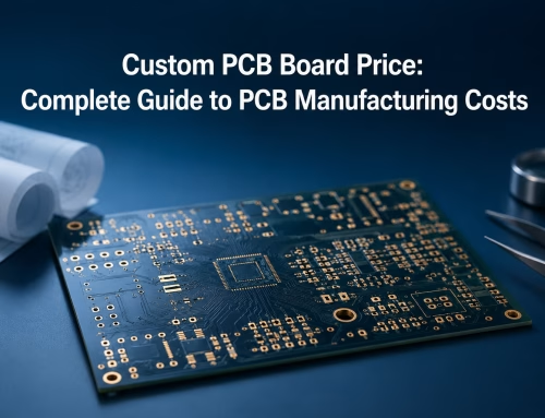
PCB is also known a printed circuit board (PCB) is a flat, non-conductive material like fiberglass, that helps connect electronic components using copper trace. These traces serve as small roads that allow electricity to flow across various components, such as capacitors, resistors and integrated circuits. Without PCBs modern electronics wouldn’t be even possible.
The process of creating PCBs is a process that involves two primary steps: PCB manufacturing assembly and component placement often referred to as assembly. Both depend on each other, each comes with its own challenge tools, processes and quality assurance.
Designing the Blueprint
Each successful PCB starts with a sketch. Engineers utilize the computer-aided designing (CAD) programs to draw the design of circuit. This digital blueprint provides specifics like where components need to be put in, the order that they will be connected and the amount of layers the board requires. The level of complexity of the project PCBs can range between one and more than twenty layers.
The design must be accurate since even a slight error could result in an unstable or malfunctioning board. The design is turned into Gerber files once it is completed. These are used by the manufacturers to build the actual board.
The Manufacturing Phase
When the design is completed then the process shifts to the hands of the printed circuit maker. The raw materials are transformed into a real PCB. The manufacturing process involves many stages, which include printing the circuit design onto copper-clad boards. Then, the etching process takes off any copper that is not needed drilling holes, the application of protective layers such as silk screens and solders masks.
This needs to be made to ensure the board meets electrical and dimensional requirements. They run quality checks like Automated Optical Inspection (AOI) and Electrical Testing to identify any errors prior to the start of the next phase. The early quality control is vital because once components are welded onto the board, repairing mistakes is much more difficult and costly.
PCB Assembly Infusing Life into the Board

Once the board is ready for assembly, the next step come PCB Manufacturing Assembly which is where the components are attached to the board in order to create a functional. This stage combines human and machine skill to attain accuracy and speed.
When it comes to assembling PCBs, Through-Hole Technology and Surface Mount are two main sources to be used. SMT is the most common type of assembly in electronics of today because it permits components to be put directly on the board. The method employs pick-and-place devices to precisely position components like diodes, resistors and microchips, based on the layout of the design.
Following the placement the board is put through a reflow process of soldering in which it is heated in an oven until the solder melts and creates electric connections to the boards and components. If the components aren’t able to withstand this type of heat or require more mechanical connections, THT is employed. This is done by inserting the leads of the component through holes that have been pre-drilled and connecting them to the other side.
Quality Control and Testing
Quality assurance doesn’t stop after the components are placed on the board. Testing is even more crucial. When it comes to testing during PCB construction process, designers employ a variety of tests to make sure all functions are functioning as they were intended. These tests comprise the In-Circuit Testing (ICT) and Functional Testing, and X-ray inspections, specifically for boards that have hidden solder joints, such as BGAs.
Every test is a check for a variety of possible issues — such as short circuits and cold solder jointsmaking sure that the final board is not just functional, but also reliable in the long run. Quality PCB assembly manufacturing concentrates as much on longevity as it is focused on performance.
Packing and Delivery
After the tests and inspections, the boards are cleaned to eliminate flux dust or other residues. The boards are then packed in accordance with the specifications of the customer in a variety of ways, including individual units, in anti-static tray or with custom packaging.
Certain manufacturers provide complete turnkey solutions, which mean they manage everything from the purchase of the components to final delivery. It is a simple process that allows users to focus on their main goals while managing PCB makers handles the production methods. Shipping and delivery is usually performed with care to the sensitivity of handling, particularly for boards that are utilized in high-performance or high-reliability settings such as aerospace or medical equipment.
Importance of Choosing the Right Partner
Selecting the right partner for manufacturing PCBs can be crucial to the success of the success of a project. Expertly-trained manufacturers offer more than just machines — they provide insight into design enhancements and sourcing options and regulatory compliance.
When you’re creating your first prototype or getting ready for mass production using the correct team guarantees efficiency, performance and peace of head.
Summary
Although the process may seem intimidating at first but understanding the flow of the process gives you a greater appreciation of the electronic components that make our world work.
It doesn’t matter if you’re a designer or engineer, or just an avid learner, understanding the process of an assembly of PCBs can help create the bridge between concepts and production. It’s more than just the process of putting parts on the board; it’s about creating the pulse of the latest technology.
In this complex process the cooperation between engineers, designers, and a highly skilled printed circuit manufacturer is what helps transform ideas into functioning possibility.

Get Quote Free