Multilayer PCBs: Advantages and Disadvantages
A comprehensive analysis of multilayer circuit board design, comparing benefits, limitations, and real-world applications across industries.
Get Your PCB Quote!
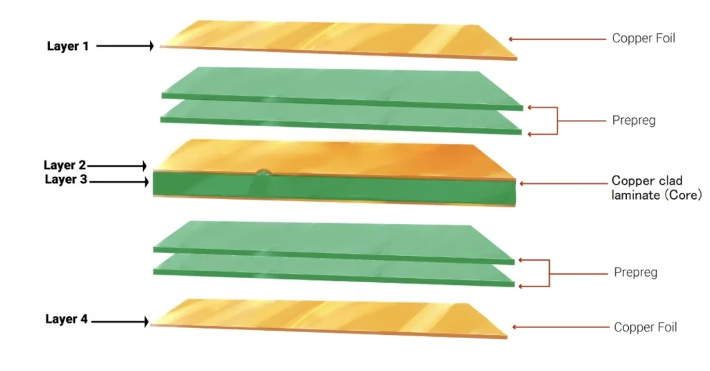
Table of Contents
Table of Contents
Advantages vs. Disadvantages
| Aspect | Multilayer PCBs | Single/Double-Layer PCBs |
| Circuit Density | High; uses vertical space | Low; limited to surface area |
| Signal Integrity | Excellent; controlled impedance & shielding | Poor; lacks dedicated return planes |
| Size & Weight | Compact & lightweight | Bulky for complex circuits |
| Design Flexibility | High; multiple routing layers | Limited |
| Manufacturing Cost | Higher (25–40% per added layer) | Lower |
| Repairability | Very difficult to impossible | Relatively straightforward |
| Thermal Management | Superior (internal heat spreading) | Limited |
| Design Complexity | High; requires expert planning | Low |
Table 1: Multilayer vs. Simple PCBs — Feature Comparison
Need PCB Manufacturing or Assembly?
Get a free quote within 24 hours. We specialize in prototype-to-production PCB/PCBA for hardware teams worldwide.
Advantages of Multilayer PCBs
Multilayer PCBs have become the industry standard for high-performance electronics due to their numerous technical and operational benefits. Below is a detailed breakdown of each advantage:
1. Higher Circuit Density & Component Integration
Multilayer design enables far more circuits and components to fit in a given footprint by utilizing vertical space. Instead of spreading connections across a single layer, engineers allocate specific layers for signals, power, and ground.
Key benefits:
- Compact design:Allows smartphone, wearable, and medical device form factors impossible with 2-layer boards
- HDI technology:Microvias (<150 µm) + fine-line routing (3 mil or less) enable 500-pin BGAs with 0.5 mm pitch to route properly
- Single unified board:Replaces multiple interconnected boards, eliminating connector failures and reducing assembly weight
2. Excellent Signal Integrity & EMI Control
One of the strongest reasons to adopt multilayer design is the ability to manage electromagnetic compatibility (EMC). Dedicated ground and power planes provide controlled return paths for signals.
| Technique | Mechanism | Performance Impact |
| Controlled Return Paths | Ground plane immediately adjacent to signal layer | EMI reduction: 12–18 dB |
| Impedance Control | Specific trace width & dielectric thickness | Achieves ±10% impedance tolerance |
| Stripline Routing | Signal layer sandwiched between two ground planes | 360° shielding; reduces crosstalk by 20–40% |
| Multiple Ground Planes | Multiple dedicated reference layers | Further noise reduction; stable voltage distribution |
Table 2: Signal Integrity Techniques in Multilayer PCBs
3. Superior Thermal Management
Heat is the enemy of component longevity. Multilayer boards distribute thermal energy far more effectively than 2-layer designs.
Thermal management strategies:
| Method | Description | Benefit |
| Thermal Vias | Connect hot component pads to internal copper planes | Reduces IC junction temperature by 10–30 °C |
| Heavy Copper Layers | 2–3 oz copper on internal layers (vs. standard 1 oz) | Increases heat-spreading capacity |
| Copper Planes as Heat Sinks | Internal power/ground planes act as thermal spreaders | Eliminates need for bulky external heatsinks |
| High-Tg Substrates | Materials with elevated glass transition temperatures (FR-4, Rogers) | Prevents delamination under thermal stress |
Table 3: Thermal Management Techniques
4. Mechanical Durability & Reliability
The layer-pressing process creates a dense, rigid composite structure more resistant to warping, vibration, and mechanical stress. This is why multilayer boards dominate automotive ECUs, industrial controls, and aerospace applications.
Durability factors:
- High-pressure lamination fuses layers into monolithic structure resistant to warping during soldering
- Internal layers shielded from environmental wear (dust, moisture, UV)
- Uniform stress distribution reduces mechanical failure risk
5. Design Flexibility & Layer Allocation
Each layer can be optimized for a specific function. Designers gain unprecedented freedom in signal routing, power distribution, and grounding strategies.
Example layer allocation (8-layer board):
- Layer 1: Top signal (high-speed differential pairs)
- Layer 2: Ground plane (primary return path)
- Layer 3–4: Buried signal routing
- Layer 5–6: Ground/Power planes
- Layer 7: Signal routing (lower-speed)
- Layer 8: Bottom signal + component mounting
6. Performance in High-Frequency Applications
Multilayer structures are essential for high-speed protocols: PCIe, USB 3.0/3.1, DDR4/DDR5, 5G, and automotive radar.
Why multilayer excels at high frequency:
- Controlled impedance prevents signal reflections
- Ground planes minimize loop inductance (critical for >1 GHz signals)
- Stripline routing offers 360° EMI shielding
Disadvantages of Multilayer PCBs
Despite their advantages, multilayer PCBs come with real tradeoffs. Understanding these limitations is crucial for making sound design decisions.
1. Significantly Higher Manufacturing Costs
Each added layer increases board cost by approximately 25–40%, driven by material, processing, and testing requirements.
| Cost Component | Impact on 4-Layer Board | Impact on 8-Layer Board |
| Raw Materials (copper, prepreg) | +30–35% | +60–75% vs. 2-layer |
| Lamination Cycles | +20% | +50% |
| Drilling & Plating | +15% | +40% |
| Testing (AOI, X-ray, Electrical) | +25% | +45% |
| Overall Cost Multiplier vs. 2-Layer | ~2.0× to 2.5× | ~3.5× to 4.5× |
Table 4: Cost Breakdown by Layer Count (Relative to 2-Layer Board)
2. Extreme Design Complexity
Multilayer design demands expert-level skills in stack-up planning, impedance control, thermal modeling, and DFM (Design for Manufacturing).
Sources of complexity:
- Stack-up design:Must balance signal integrity, power distribution, thermal management, and mechanical strength
- Impedance modeling:Requires detailed understanding of dielectric constants, trace dimensions, and layer spacing
- Routing constraints:Dense placement of thousands of signals on 6–8 layers requires sophisticated CAD tools and experience
- Iteration time:Design reviews, simulations, and layout corrections can extend timelines by months
3. Extremely Difficult Repairs & Debugging
Once a multilayer board is manufactured, fixing internal defects is nearly impossible without destroying the board.
Repair limitations:
- Hidden defects:Inner-layer shorts or opens cannot be accessed without delaminating the board
- X-ray inspection required:Diagnosing internal faults requires expensive X-ray equipment and specialized expertise
- No blue-wiring fix:Unlike 2-layer prototype boards, hand-soldered jumpers are impractical at high trace densities
- Complete replacement:Most manufacturing defects require scrapping the board, not just the failed component
4. Manufacturing Yield & Registration Challenges
Precise layer alignment is critical. Even microscopic misalignment can cause failures.
Manufacturing risks:
- Layer alignment tolerance:Typically ±5 µm; excessive shift causes vias to miss pads
- Via registration failures:Misaligned blind/buried vias create open circuits
- Yield loss:Complex stackups may achieve only 85–92% yield, vs. 98%+ for 2-layer boards
- Scrap cost:A single misregistered 8-layer board represents 8× the material waste of a 2-layer
5. Extended Design & Manufacturing Timeline
The complexity of multilayer design and manufacturing significantly extends project schedules.
| Phase | 2-Layer Board | 6-Layer Board | 12-Layer Board |
| Design & Simulation | 2–3 weeks | 6–8 weeks | 10–14 weeks |
| Design Review & Iteration | 1–2 weeks | 3–4 weeks | 4–6 weeks |
| Prototype Fabrication | 1 week | 2–3 weeks | 3–4 weeks |
| Testing & Debugging | 2–3 weeks | 4–6 weeks | 6–8 weeks |
| Total Project Timeline | 6–8 weeks | 15–21 weeks | 23–32 weeks |
Table 5: Typical Project Timeline by PCB Complexity
6. Thermal Concentration Risk (If Poorly Designed)
While multilayer boards excel at heat spreading, poor stackup design can actually trap heat in interior layers.
Potential issues:
- Inadequate thermal vias → hot spots on high-power ICs (>5 W)
- Thick FR-4 dielectric layers → reduce thermal conductivity
- Dense component placement → insufficient air gaps for convection cooling
- Requires active cooling (fans) in compact designs → adds cost & power consumption
Head-to-Head Comparison: Should You Use Multilayer?
| Decision Factor | Use Multilayer PCB | Stick with 2-Layer |
| Signal speeds | >100 MHz or high-speed protocols (PCIe, USB 3.0, DDR4) | <100 MHz, basic digital logic |
| Component density | BGA with >100 pins, HDI designs | <50 total components, through-hole only |
| Thermal dissipation | Components >2 W each, compact form factor | <0.5 W total power, open layout |
| EMI requirement | Stringent (medical, telecom, aerospace) | Basic consumer electronics |
| Project budget | $50k–$500k+ development cost acceptable | Cost-sensitive, budget <$10k |
| Time to market | 6–12 months development ok | Need to launch in 4–8 weeks |
| Production volume | Medium to high (>10k units/year) | Very low (<5k units), prototyping |
| Industry | Telecom, automotive, medical, aerospace | Hobby, simple appliances, toys |
Table 6: Quick Decision Matrix
Real-World Applications by Industry
Here’s where multilayer PCBs are non-negotiable:
| Industry | Typical Application | Typical Layer Count | Key Requirement |
| Telecommunications | 5G base stations, cellular routers | 10–40+ layers | Signal integrity at GHz frequencies |
| Automotive | ADAS systems, EV battery management (BMS) | 6–12 layers | Reliability under thermal/mechanical stress |
| Medical Devices | MRI machines, portable ultrasound, ECG monitors | 6–8 layers | EMI shielding + signal fidelity for diagnostics |
| Consumer Electronics | Smartphones, laptops, gaming devices | 6–10 layers | Miniaturization + heat dissipation |
| Aerospace & Defense | Flight control systems, radar electronics | 8–16 layers | Durability, compact, vibration-resistant |
| Industrial Control | PLCs, robotics, factory automation | 4–8 layers | Reliability under harsh environmental conditions |
| High-Frequency RF | Satellite communications, radar systems | 6–10 layers + Rogers/PTFE substrate | Minimal signal loss, controlled impedance |
Table 7: Industry Applications of Multilayer PCBs
Cost Optimization Strategies
Multilayer PCBs are expensive, but smart design can reduce costs without sacrificing performance:
1. Minimize Layer Count Through Efficient Design
- Use 4 layers instead of 6:If signal density allows, a 4-layer board (top signal, ground, power, bottom signal) may be sufficient
- Optimize via placement:Fewer vias → faster manufacturing, lower risk of registration errors
2. Select Appropriate Materials
- FR-4 for standard applications:Adequate for <5 GHz, costs ~30% less than Rogers
- High-frequency materials only when needed:Reserve Rogers/PTFE for RF circuits; use FR-4 for digital sections
3. Batch Production & Design Reuse
- Economies of scale:Manufacturing 1,000 units reduces per-unit cost by 20–35% vs. 100 units
- Library modules:Reuse proven subsystem designs to shorten design time and reduce errors
4. Partner with Experienced Manufacturers
- DFM consultation:Good manufacturers offer free Design for Manufacturing (DFM) reviews, catching expensive mistakes early
- Standard stackups:Using common layer configurations (4/6/8 layer) has faster lead times and lower NRE costs
How to Decide: Multilayer or Not?
Use this framework to make an informed decision:
Step 1: Evaluate Technical Requirements
- Maximum signal frequency: > 100 MHz → need multilayer
- Number of components: > 100 parts → likely need >4 layers
- Power dissipation: > 5 W → thermal management essential
- Physical footprint: < 50 cm² for complex circuit → multilayer mandatory
Step 2: Assess Project Constraints
- Development budget available?
- Timeline flexibility (6+ months for multilayer, 2–4 weeks for 2-layer)?
- Production volume (>10k units benefits from multilayer economies)?
Step 3: Prototype & Validate
- If uncertain, prototype with 4-layer board first (acceptable cost, good margin vs. 2-layer)
- Use simulations (HyperLynx, ADS, ANSYS) to validate performance before committing to manufacturing
Frequently Asked Questions
Q: What is the minimum layer count for a real multilayer PCB?
A: Technically 3 layers, but practically 4 layers is the entry point for EMI control. A 4-layer stackup (top signal, ground, power, bottom signal) provides dedicated return paths and power distribution at reasonable cost.
Q: Can I use a 2-layer board for high-speed signals (>100 MHz)?
A: Theoretically yes, but practically no. Without a ground plane, return current loops are enormous, causing EMI failures and signal reflections. It’s almost always cheaper to move to 4 layers than to over-engineer a 2-layer design.
Q: How much more does a 6-layer board cost compared to a 4-layer?
A: Approximately 25–40% more per added layer. A 6-layer board costs roughly 1.5–1.75× the price of a comparable 4-layer board. Cost per unit decreases significantly at production volumes >10k.
Q: What surface finish should I use for multilayer PCBs?
A: ENIG (Electroless Nickel Immersion Gold) is best for fine-pitch BGAs and high-reliability applications. HASL is cost-effective for standard designs. OSP is eco-friendly and suitable for high-density boards if soldered quickly after fabrication.
Q: Can I repair a broken trace on an internal layer?
A: No. Internal defects are inaccessible and typically require scrapping the entire board. This is why X-ray inspection during manufacturing is critical—it catches defects before assembly.
Q: How does a 12-layer board compare to a 6-layer in terms of performance?
A: A 12-layer board offers more routing flexibility, better thermal distribution, and improved EMI performance. However, the jump in cost and design complexity often doesn’t justify the benefit unless you have very high signal density (>1,000 traces) or extreme thermal requirements.
Q: What’s the typical lead time for a multilayer PCB prototype?
A: 2–4 weeks for 4–6 layer boards from experienced manufacturers. 12+ layer boards may take 4–6 weeks due to additional process steps (blind/buried via drilling, X-ray inspection). RUSH services (1–2 week delivery) available at 20–40% premium cost.
Q: Do I need specialized CAD software for multilayer design?
A: Professional multilayer design requires CAD tools like Altium Designer, Cadence Allegro, or KiCad with proper library management. These tools handle layer stackup definition, impedance simulation, and design rule checks essential for multilayer success.
Q: What is the most common layer count in industry?
A: 4, 6, and 8 layers dominate. These counts balance cost, performance, and supply chain maturity. Most component manufacturers provide reference designs targeting 4–8 layer stackups, making design time shorter and DFM risks lower.
Conclusion
Multilayer PCBs are not a luxury—they are a necessity for any modern, high-performance electronic device. The advantages in signal integrity, miniaturization, and thermal management far outweigh the disadvantages for applications demanding reliability and performance.
Key takeaways:
- Technical threshold:Above ~100 MHz signal speeds or high component density, multilayer design is almost always required
- Cost vs. benefit:Yes, multilayer costs 2–4× more to develop, but a failed single-layer design costs infinitely more
- Design expertise:Hire experienced multilayer designers or partner with knowledgeable manufacturers to avoid costly mistakes
- Prototype early:Validate performance with simulations and prototype boards before committing to high-volume manufacturing
The industries leading electronics innovation—telecommunications, automotive, medical, aerospace—have collectively made multilayer PCBs the de facto standard. Your product requirements, not your budget concerns, should drive this decision. In most cases, the question isn’t whether to use multilayer, but how many layers you truly need.

Get Quote Free