What is PCB Dielectric Constant (Dk)?A Complete Guide for High-Speed Board Design
Datasheet Dk values don't reflect real-world PCB behavior. Learn how frequency, moisture, glass weave, and copper roughness shift your dielectric constant — and how to build stackups that actually hit target impedance.
Get Your PCB Quote!
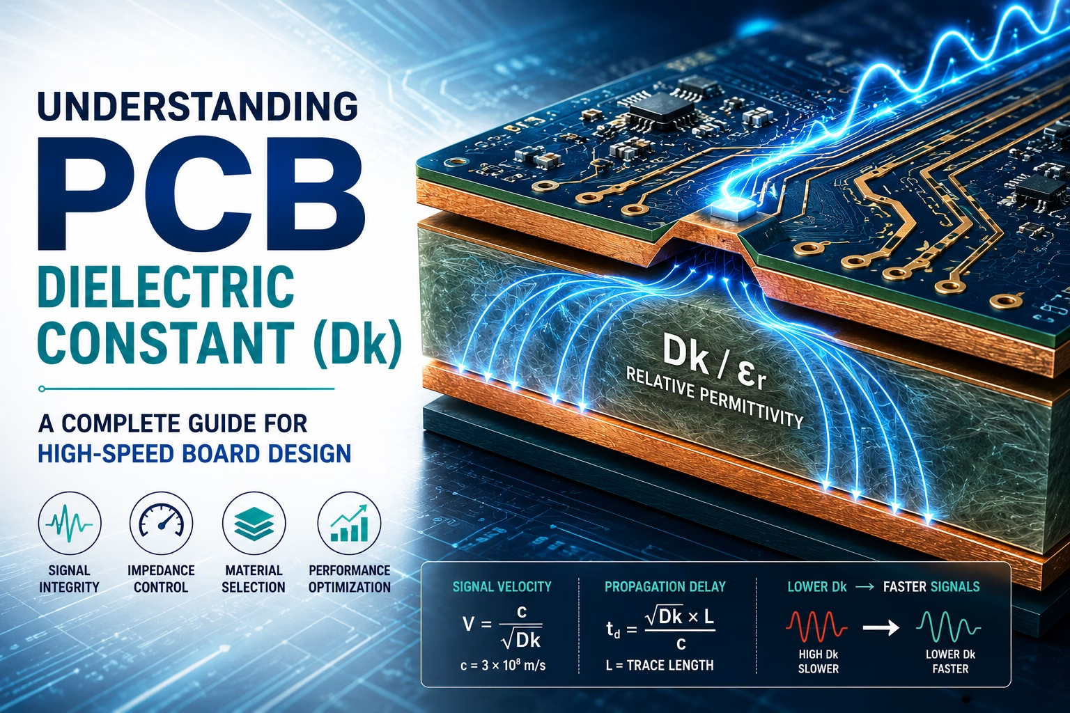
Table of Contents
1. Introduction
If you have ever run a time-domain reflectometry (TDR) test on a prototype board only to find your 50Ω transmission lines measuring at 44Ω, you have experienced the gap between datasheet Dk values and real-world performance. After 15 years of debugging high- speed stackups, I have learned that treating the dielectric constant as a static number is one of the most expensive mistakes a designer can make.
In this article, I will explain why this parameter varies so dynamically and show you how to design your board around its real-world behavior.
2. What Dk Actually Represents in a PCB Substrate
The dielectric constant (Dk), or relative permittivity (εr), measures a material’s ability to store electrical energy within an electric field relative to a vacuum. A vacuum has a Dk defined as exactly 1.0. Any physical PCB substrate contains atoms and molecules that polarize when exposed to an electric field, which concentrates the electric flux and increases the capacitance of nearby conductors. This charge-storing behavior occurs through three primary polarization mechanisms at the molecular level:
- Electronic Polarization:The rapid displacement of electron clouds relative to their nuclei. This mechanism is extremely fast and remains active well into optical frequencies.
- Ionic Polarization:The displacement of positive and negative ions relative to each other within the molecular lattice. This is highly relevant in ceramic-filled substrates.
- Dip olar (Rotational) Polarization:The physical alignment of permanent molecular dipoles with the alternating electric field. This mechanism dominates in organic polymer resins (such as epoxy) but is relatively slow. As operating frequencies increase, these large dipoles cannot keep up with the rapidly alternating field, causing a drop in energy storage capacity and a subsequent decrease in Dk.
For PCB designers, Dk is the physical parameter that dictates two non-negotiable electrical properties: the speed at which an electromagnetic wave propagates along a trace, and the characteristic impedance of that trace. Signals do not travel through the copper itself; they travel as electromagnetic waves through the dielectric medium surrounding the copper. The propagation velocity (V) is calculated using the following equation:
V = c / √Dk
Where “c” is the speed of light in a vacuum (approximately 3 × 10⁸ meters per second, or 11.8 inches per nanosecond). In a typical FR-4 laminate with a D k of 4.3, the propagation speed drops to approximately 5.7 inches per nanosecond (1. 44 × 108 m/s). In a lower-Dk material like PTFE (Dk ≈ 2.1), the velocity rises to 8.1 inches per nanosecond. When managing timing-critical interfaces like DDR4/DDR5 or high-speed PCIe Gen 5/6 lanes, precise knowledge of this velocity is mandatory for matching propagation delays across different routing layers.
Need PCB Manufacturing or Assembly?
Get a free quote within 24 hours. We specialize in prototype-to-production PCB/PCBA for hardware teams worldwide.
3. Why the “Constant” in Dielectric Constant Is a Myth
The term “dielectric constant” is a misnomer. In actual operating environments, Dk is a dynamic variable that changes in response to frequency, temperature, moisture, and material composition.
Frequency Dispersion
Because molecular dipoles require a finite time to realign with an alternating electric field, the measured Dk of any laminate decreases as the operating frequency increases. This phenomenon is known as frequency dispersion. A standard FR-4 laminate that exhibits a Dk of 4.7 when tested at a static 1 MHz frequency will often drop to 4.3 at 1 GHz, and fall further to 4.15 at 10 GHz.
If you perform transmission line calculations using the 1 MHz datasheet value for a 5 GHz digital signal, your trace width calculations will be off. The target 50Ω transmission line will end up with an actual impedance significantly higher than simulated, resulting in unwanted reflections and degraded signal margins.
Temperature and Moisture Effects
Laminates exhibit a thermal coefficient of dielectric constant (T_c D_k), which quantifies how much the Dk shifts per degree Celsius of temperature change. For many standard materials, Dk increases as temperature rises because the polymer matrix expands, allowing greater molecular mobility and stronger dipolar alignment. This is a critical factor for aerospace or automotive designs where the operating envelope spans from -40°C to +125°C.
Moisture absorption poses an even larger risk. Water has an incredibly high dielectric constant of approximately 80 at room temperature . If a PCB substrate absorbs even 0.1% to 0.2% moisture by weight due to ambient humidity , the overall composite Dk will spike. This shift changes trace impedance and increases the dissipation factor (Df), which exponentially drives up dielectric loss.
Anisotropy in PCB Laminates
PCB laminates are composite structures constructed from woven fiberglass fabric embedded in an organic resin matrix. Woven glass fibers typically have a Dk of 6.6 to 7.2, while the surrounding epoxy resin has a Dk of 3.0 to 4.0 . Because of this composite nature, laminates are anisotropic: their electrical properties are different depending on the direction of the electric field.
Most material suppliers measure and report Dk along the Z-axis (out-of-plane, through the thickness of the board) because this is easiest to test in a laboratory. However, the electromagnetic fields of micro strip and stripline traces propagate along the X and Y axes (in-plane). This discrepancy can introduce a 3% to 5 % error in your impedance models if your software simulation assumes isotropic material properties.
4. How Dielectric Constant Governs Your Trace Geometry and Signal Speed
The relationship between Dk and trace geometry is governed by the boundary conditions of electromagnetic fields. To maintain a target characteristic impedance (typically 50Ω for single-ended traces or 100Ω for differential pairs), the ratio of the trace width (W) to the dielectric thickness (H) must balance the trace’s self-inductance against its capacitance to the reference plane.
When you select a laminate with a higher Dk, the capacitance per unit length increases. To restore the balance and maintain your target impedance, you must decrease the trace width to reduce that capacitance. Conversely, a lower-Dk material stores less energy, requiring a wider trace to achieve the same capacitance and characteristic impedance target.
Let’s look at a concrete design scenario. Suppose we are designing a 50Ω microstrip line on a 4-mil (0.101 6 mm) dielectric thickness over a solid ground plane.
- If we use a standard, high -loss FR-4 core with a Z-axis Dk of 4.30, the required trace width is approximately 7.5 mils (0.190 mm).
- If we transition the design to a low-loss Rogers RO4350B hydrocarbon/ceramic laminate with a Z-axis Dk of 3.66, the required trace width increases to 8.8 mils (0.223 mm).
This geometry shift has significant downstream manufacturing and performance impacts:
| Laminate Parameter | Standard FR-4 (Dk 4.30) | Rogers RO4350B (Dk 3.66) | Impact on Performance & Manufacturing |
| Target Impedance | 50Ω ± 10% | 50Ω ± 5% | Tightened tolerances improve high-speed channel margin. |
| Required Trace Width | 7.5 mils (0.190 mm) | 8.8 mils (0.223 mm) | Wider traces are less sensitive to etching variation during fabrication. |
| Conductor Loss (Skin Effect ) | Higher | Lower | W ider trace surface area reduces skin effect resistance at high frequencies. |
| Propagation Delay | 175 ps / inch | 1 62 ps / inch | Faster propagation reduces latency and tightens timing margins. |
I once spent three weeks troubleshooting a 10 GHz RF board where the fabricator substituted a generic FR-4 core with 7628-style glass weave (Dk ≈ 4.60) for the specified low-resin core (Dk ≈ 4.10) to save processing time. The resulting 43 Ω impedance mismatch completely destroyed the return loss on our input low-noise amplifier, forcing an immediate, expensive scrap and rebuild of the entire prototype batch.
5. Why Different Dk Measurement Methods Yield Conflicting Results
One of the most frustrating challenges in high-frequency design is that different industry-standard test methods yield different Dk values for the exact same piece of material. If you compare a laminate’s Dk from two different datasheets, you must verify the test methodologies used to obtain those numbers.
The IPC recognizes several test methods under IPC-TM-65 0, each employing a unique electromagnetic field configuration that interacts with the material’s anisotropy in different ways.
IPC-TM-650 Stripline Resonator (Method 2.5.5.5)
The stripline resonator method is the workhorse of the laminate industry and the source of most published datasheet values. This method clamps an unclad card of the material under test between two ground planes, using a copper foil resonator pattern positioned in the center. The vector network analyzer (VNA) measures the resonant frequencies of this structure.
- Field Orientation :Purely Z-axis (perpendicular to the laminate sheets).
- Advantage:Highly repeatable and excellent for raw material quality control.
- Limitation:Does not account for copper surface roughness since it uses a clamped, non-bonded copper foil. This often yields a “Process Dk” that is lower than the actual ” Design Dk” experienced by an etched PCB trace.
Split-Post Dielectric Resonator (SPDR)
The SPDR method places a flat sheet of unclad laminate into a gap between two precisely machined dielectric resonators . It measures the shift in the resonant frequency and the change in the quality factor (Q) caused by the introduction of the sample.
- Field Orientation:In-plane (X-Y axis), parallel to the laminate surface.
- Advantage:Highly accurate and completely non-destructive. Excellent for thin materials.
- Limitation:Sensitive to material thickness variations. Because the electric field is in-plane, it will measure a different Dk than Z-axis methods due to material anisotropy.
Full-Sheet Resonance (FSR)
FSR uses a fully copper-clad laminate panel itself as a parallel-plate resonator. The panel is excited at its edges, and the resonant frequencies are measured .
- Field Orientation:Z-axis.
- Advantage:Fast, non-destructive, and characterises the entire production panel.
- Limitation:Does not capture local variations or high-frequency dispersion patterns, as it is typically limited to lower frequency modes.
Transmission Line Methods (TDR/VNA)
Rather than testing raw material in a cavity, transmission line methods extract directly from a fabricated PCB test coupon. A known transmission line structure (typically a microstrip or stripline) is excited, and the propagation delay or phase shift is measured across a wide frequency sweep.
- Field Orientation:A combination of Z-axis and in-plane fields, matching actual operating conditions.
- Advantage:Capt ures the “effective Dk” (), which includes the physical impacts of copper roughness, l amination press cycles, and adhesive prepreg flows. This is the value that your 3D field solvers need for accurate routing simulations.
- Limitation:Highly destructive and expensive, as it requires dedicated fabrication of test structures .
| Measurement Method | IPC Test Method Reference | Primary Axis Measured | Sample Condition Required | Best Use Case |
| Clamped Stripline Resonator | IPC-TM-650 2.5 .5.5 | Z-Axis | Unclad card (clamped) | Laminate manufacturer quality control & raw material sorting. |
| Split-Post Resonator (SPDR) | IPC-TM-650 2.5.5 .13 | X-Y Plane (In-Plane) | Unclad sheet (loose insertion) | Ultra-precise material characterization for thin, low-loss sheets. |
| Full-Sheet Resonance (FSR) | IPC-TM-650 2.5 .5.6 | Z-Axis | Double-sided copper clad sheet | Incoming material inspection at PCB fabricators. |
| Transmission Line (TDR/VNA) | IPC-TM-650 2.5.5.12 | Mixed (Z-Axis & X -Y Plane) | Fabricated PCB Test Coupon | Impedance modeling validation & Design Dk extraction. |
6. The Crucial Interaction Between Dk, Resin Content, and Glass Weave
Because PCB laminates are heterogeneous composites, the glass style you specify has a direct and immediate impact on the laminate’s Dk and your overall signal integrity.
Resin-to-Glass Ratio
Glass styles are designated by standard industry numbers (such as 106, 1080, 2116, or 7628) which define the physical yarn diameter, thread count, and weave density of the fiberglass fabric. F iner fabrics like 106 have low glass content and high resin content (often greater than 70% resin by weight). Coarser fabrics like 7628 have high glass content and low resin content (often around 40%).
Because epoxy resin has a much lower Dk (typically 3.2 to 3.6 ) than fiberglass (typically 6.6 to 7.2), a laminate made with 106 glass will have a significantly lower composite Dk than a laminate of the same overall thickness made with 7628 glass. Fabricators regularly alter the resin content of their prepregs to hit specific thickness targets, but if they do not adjust the Dk values in their stackup generator accordingly, your impedance calculations will fail.
| Glass Style | Nominal Cured Thickness | Typical Resin Content (%) | Typical Composite Dk (at 1 GHz) | Glass Weave Density Class |
| 106 | 1.5 mils (0.038 mm) | 75% | 3.70 – 3.85 | Ultra-Open We ave |
| 1080 | 2.5 mils (0.064 mm) | 65% | 3.90 – 4 .05 | Open Weave |
| 2116 | 3.8 mils (0. 097 mm) | 55% | 4.15 – 4.30 | Medium Weave |
| 7628 | 6.8 mils (0.173 mm) | 44% | 4.40 – 4.60 | Dense Weave |
The Glass Weave Effect and Phase Skew
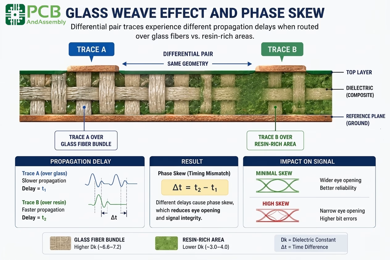
In standard open-weave fabrics like 106 or 1080, there are substantial physical gaps between the woven glass bundles. These gaps are filled entirely with pure epoxy resin. When a differential pair is routed across this substrate, one conductor of the pair may run directly over a dense glass bundle (Dk ≈ 6.6), while the companion conductor runs directly over a resin-rich gap (Dk ≈ 3.2).
Because the signal velocity is inversely proportional to √Dk, the signal traveling over the resin pocket propagates significantly faster than the signal traveling over the glass bundle. Over a 10-inch trace, this local velocity mismatch can introduce substantial phase skew:
- Trace A (over glass): Effective Dk ≈ 4.20 . Propagation delay ≈ 173 ps/inch. Total delay ≈ 1. 73 ns.
- Trace B (over resin): Effective Dk ≈ 3.60. Propagation delay ≈ 161 ps/inch. Total delay ≈ 1.6 1 ns.
- Total Skew ≈ 120 ps.
At 28 Gbps, a single bit’s duration (unit interval) is only 35.7 picoseconds. A 120 ps skew destroys the differential signal’s phase relationship, closing the eye diagram and causing complete data transmission failure. To prevent this, high-speed designers must specify flat, spread-glass fabrics (such as 1067, 1078, or 3313) where the glass fibers are mechanically flattened to eliminate open resin pockets, ensuring a uniform Dk environment across all traces.
How Copper Surface Roughness Artificially Inflates Dk
At high operating frequencies, current is forced to flow in a very thin layer near the outer boundary of the copper conductor due to the skin effect. If the copper surface is rough, the electromagnetic wave is forced to follow the micro-contours of the copper peaks and valleys. This slows down the propagation of the wave, acting like a slow-wave structure.
When you measure the propagation delay of this transmission line, the slow-down makes the dielectric material behave as if it has a higher D k than its true bulk material properties. This is called the “effective Dk” or “perceived Dk.” To prevent impedance mismatches at frequencies above 5 GHz, you must select laminates that use low-profile copper foils, such as Very Low Profile (VLP) or Hyper-Very Low Profile (HVLP) copper, which feature a surface roughness ( Rz) of less than 1.5 µm.

About OrinewPCB
Time is money in your projects – and OrinewPCB gets it. OrinewPCB is a PCB assembly company that delivers fast, flawless results every time. Our comprehensive PCB assembly services include expert engineering support at every step, ensuring top quality in every board. As a leading PCB assembly manufacturer, we provide a one-stop solution that streamlines your supply chain. Partner with our advanced PCB prototype factory for quick turnarounds and superior results you can trust.
7. Selecting the Right Substrate: Rogers vs . High-Tg FR-4
When selecting PCB laminates, you must balance electrical performance, thermal reliability , manufacturability, and cost. There is no single “best” material, but there are clear thresholds where continuing to use cheap, standard FR-4 becomes a massive risk.
When a design moves past 5 GHz or requires multi-gigabit data lanes (such as PCIe Gen 4/5 or 100G Ethernet), I advise clients to transition away from standard, high-loss FR-4. For projects with tight budgets that cannot tolerate pure PTFE or Rogers pricing, I recommend middle-ground materials like Isola FR408HR or Panasonic Megtron 6. These laminates utilize modified epoxy-PPE resins and low-Dk glass to deliver a much tighter Z-axis Dk tolerance ( typically ±0.05) and a dissipation factor below 0.005, preserving signal amplitude over long trace runs without driving manufacturing costs to extremes.
| Laminate Class | Example Materials | Nominal D k (at 10 GHz) | Nominal Df (at 10 GHz) | Optimal Frequency Range | Relative Material Cost Factor |
| Standard FR-4 | Isola 370HR, IT- 180A | 4 .10 – 4.30 | 0.0150 – 0.0220 | DC to 2 GHz | 1.0x (Baseline ) |
| Mid-Loss / High-Speed | Isola FR408 HR, Nelco N4000-13 | 3.60 – 3.80 | 0.0080 – 0.0100 | 2 GHz to 8 GHz | 1.5x – 2.0x |
| Ultra-Low Loss (PPE /PPO) | Panasonic Megtron 6, Megtron 7 | 3.30 – 3.40 | 0.0020 – 0.0 040 | 8 GHz to 30 GHz | 2.5x – 3.5x |
| PTFE / Ceramic RF | Rogers RO4350B, RO3003 | 3.00 – 3.66 | 0.0010 – 0.0030 | 10 GHz to 80+ GHz | 4.5x – 8.0x |
High-Tg (glass transition temperature) is not the same as low-loss. High-Tg refers to the temperature at which the resin shifts from a rigid, glassy state to a soft, rubbery state during thermal cycling. While a high-Tg material like Isola 370HR (Tg = 180°C) is highly mechanically reliable during reflow soldering, its electrical performance (Dk ≈ 4.2, Df ≈ 0.018) is still equivalent to standard FR-4. Do not make the common mistake of assuming a “high-Tg” label guarantees signal integrity at gigahertz speeds.
8. How to Build a Fail-Safe High-Speed Stackup
To avoid impedance mismatches and layout errors during production, you should follow a structured, multi-step process when modeling your PCB stackup:
- Engage Your Fabricator Early:Never design a stackup in isolation based on default values from an online calculator or a generic CAD library . Always contact your fabricator first and request their “bonded stackup sheet,” which reflects their actual inventory of cores, prepregs , and copper foils.
- Use “Design Dk” Instead of “Process Dk”:Ensure that your impedance calculation tools are configured with the frequency-dependent “Design Dk” value of the material, not the 1 MHz raw material test value. Field solvers like Polar Si9000 or Simbeor require the exact cured thickness and resin -glass ratios to output precise trace widths.
- Specify Spread-Glass Fabric Styles:To eliminate phase skew on differential pairs, explicitly write on your fabrication drawing: “All high-speed layers must use mechanically spread glass prepreg styles (e.g., 1067, 1078, 3313 ). Standard open-weave glass (e.g., 106, 1080) is prohibited on signal layers.”
- Account for Copper Roughness:If you are simulating channels operating above 10 Gb ps (or 5 GHz Nyquist), make sure your field solver utilizes a proper copper roughness model (such as the Hur ay or Hammerstad-Bekenyi models) to account for the artificial increase in effective Dk caused by the copper profile.
- Design for Hybrid Stackups:If your board contains only a few high-frequency lines (such as a 24 GHz radar antenna feed or a 10 Gbps transceiver), you can control costs by using a hybrid stack up. This technique places a premium, low-loss material (like Rogers RO4350B) on the outer layers to carry the critical signals, while utilizing cheaper FR-4 for the internal low-speed digital and power layers.
9. FAQ
Q: Are dielectric constant and relative permittivity the exact same concept?
A: Yes. In electronic engineering, “dielectric constant (Dk)” and “relative permittivity (& epsilon;r)” are used interchangeably to describe a material’s capability to store electric charge relative to a vacuum.
Q: What is the difference between Dk and Df in PCB materials?
A: The dielectric constant (Dk) measures how much the material slows down signals and affects impedance. The dissipation factor (Df), also called loss tangent, measures how much signal energy is converted to heat as it passes through the material. While Dk affects impedance and propagation delay, Df directly impacts signal attenuation. For high-frequency applications, both must be low—Dk for proper impedance control and Df for minimal signal loss.
Q: Does copper roughness influence the measured Dk?
A: Yes. High-frequency electromagnetic waves travel near the surface of the copper. Rough copper forces the wave to follow a longer , more tortuous path, which slows the propagation velocity. When this delay is measured, the system interprets it as a higher effective Dk.
Q: What Df value is acceptable for a high-speed channel running at 28 Gbps?
A: For 28 Gbps Ser Des routing, you should select laminates with a dissipation factor (Df) of 0.0035 or lower at the target Nyquist frequency (14 GHz). Using standard FR-4 (Df ≈ 0. 015) over a 5-inch channel at this speed will result in excessive attenuation and signal loss.
Q: Why does Dk decrease slightly as the frequency increases?
A: This occurs due to the physical limitations of molecular polarization. At low frequencies, molecular dipoles can align completely with the alternating electric field. As the frequency climbs into the gigahertz range, these larger dipoles cannot rotate fast enough to keep pace with the field, reducing the material ‘s overall charge storage capability.
Q: Is a lower Dk always better for RF antenna design?
A: Not necessarily. While a lower Dk reduces dielectric losses and increases radiation efficiency, a higher Dk effectively shortens the electrical wavelength. This allows RF engineers to design much smaller resonant antenna elements and highly compact microwave filters.
Q: Is Rogers material always better than FR4 for high-frequency designs?
A: Not always. Rogers materials excel in RF and microwave applications where their low Dk, ultra-low loss, and tight Dk tolerance are essential. However, they cost 5-15× more than FR4 and can be harder to manufacture. For applications below 3-5 GHz where modest signal loss is acceptable, high-performance FR4 variants (like Isola 370HR or FR408HR) often provide sufficient performance at much lower cost. The right choice depends on your specific frequency, loss budget, and cost constraints.
10. Summary
If you want your high-speed designs to work on the first spin, stop designing with nominal values. Demand the exact glass style , resin content, and frequency-dependent Dk data from your fabricator’s stackup engineer before you route a single trace. The extra two hours spent aligning these parameters saves thousands of dollars in optical inspection, debug time, and unnecessary board spins later.

Get Quote Free