How to Choose PCB Stencil Thickness for PCB Assembly
A practical guide to selecting the right PCB stencil thickness — covering IPC-7525 Area Ratio, step stencils, and common mistakes to avoid in SMT assembly.
Get Your PCB Quote!
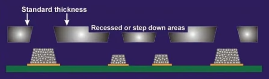
Table of Contents
- What Is PCB Stencil Thickness and Why Does It Matter?
- Standard Stencil Thicknesses and When to Use Each
- The Two Engineering Rules That Govern Stencil Design (IPC-7525)
- Step Stencils: When One Thickness Isn’t Enough
- Stencil Manufacturing Methods: Laser-Cut vs. Electroformed vs. Chemically Etched
- Common Stencil Thickness Mistakes
- Frequently Asked Questions
- Conclusion
Table of Contents
- What Is PCB Stencil Thickness and Why Does It Matter?
- Standard Stencil Thicknesses and When to Use Each
- The Two Engineering Rules That Govern Stencil Design (IPC-7525)
- Step Stencils: When One Thickness Isn’t Enough
- Stencil Manufacturing Methods: Laser-Cut vs. Electroformed vs. Chemically Etched
- Common Stencil Thickness Mistakes
- Frequently Asked Questions
- Conclusion
Stencil thickness is one of the most overlooked variables in the PCB assembly process — yet it directly determines solder paste volume, which controls joint reliability, bridging risk, and first-pass yield. Get it right and your boards assemble smoothly. Get it wrong, and you’ll chase tombstoning, insufficient solder, and shorts across an entire production run.
This guide covers how stencil thickness works, the engineering rules that govern it, and how to select the right thickness for your specific component mix.
Key Takeaways
- Stencil thickness controls solder paste volume — the single most important variable in SMT yield
- IPC-7525 defines two critical ratios: Aspect Ratio (min 1.5) and Area Ratio (min 0.66) for reliable paste release
- 5 mil (0.125 mm) is the industry standard for mixed-component boards; adjust thinner for fine-pitch and thicker for power components
- Step stencils solve mixed-thickness requirements on a single board but add cost and lead time
- The quality of a manufacturer’s stencil-related DFM feedback reveals their process engineering maturity
What Is PCB Stencil Thickness and Why Does It Matter?
A PCB stencil is a precision laser-cut metal sheet (typically stainless steel) used to deposit solder paste onto PCB pads during the SMT printing process. The stencil sits on top of the PCB, solder paste is applied across its surface, and a squeegee forces paste through the apertures (holes) onto the pads below.
Stencil thickness defines the z-axis of the deposited paste volume. Combined with aperture dimensions, it determines exactly how much solder ends up on each pad.
The consequences of incorrect thickness are significant:
| Thickness Issue | Result | Common Defects |
| Too thick | Excess solder paste | Bridging, shorts, solder balls, BGA solder ball collapse |
| Too thin | Insufficient solder paste | Weak joints, open circuits, head-in-pillow (BGA), tombstoning (passives) |
The correct thickness delivers the right paste volume for every component on the board — enough to form a reliable joint without risking shorts.
Standard Stencil Thicknesses and When to Use Each
Most PCB assemblies fall into one of five standard thickness ranges. The choice depends primarily on your component mix, with the finest-pitch components dictating the upper bound.
| Thickness | Best For | Component Types | Common Applications |
| 3–4 mil (0.075–0.10 mm) | Ultra-fine pitch | 01005, 0201, 0.3–0.4 mm pitch BGA/QFN | Miniaturized designs, mobile devices, wearables |
| 5 mil (0.125 mm) | Mixed-component boards | 0402, 0603, 0.5 mm pitch BGA/QFN | Industry standard — most general-purpose assemblies |
| 6 mil (0.15 mm) | Standard + larger components | 0805, 1206, SOIC, QFP (0.5 mm+ pitch) | Industrial controls, power supplies |
| 7–8 mil (0.175–0.20 mm) | Large components, power devices | Connectors, thermal pads, inductors, TO-252 | High-current designs, LED boards, power modules |
5 mil Is the Default — Here’s Why
5 mil (0.125 mm) is the industry standard for a reason. It provides sufficient paste volume for common 0.5 mm pitch components while remaining thin enough to avoid bridging on 0402 and 0603 passives. For a typical board with a mix of standard passives, QFPs, and 0.5 mm pitch BGAs, 5 mil is the right starting point.
When to deviate from 5 mil:
- Your board uses 0201 or smaller passives → consider 4 mil
- Your board uses 0.4 mm or finer pitch BGAs → consider 4 mil or step stencil
- Your board has large thermal pads or power components requiring high solder volume → consider 6–8 mil
- Your board has both ultra-fine-pitch AND high-volume components → consider a step stencil (see below)
The Two Engineering Rules That Govern Stencil Design (IPC-7525)
IPC-7525 is the industry standard for stencil design. It defines two critical ratios that determine whether solder paste will reliably release from the stencil aperture onto the PCB pad.
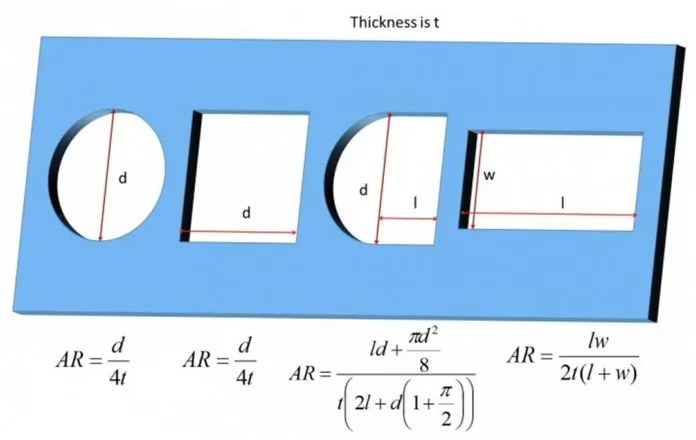
Aspect Ratio (AR)
Aspect Ratio = Aperture Width / Stencil Thickness
Minimum acceptable value: 1.5
The aspect ratio ensures the paste physically fits through the aperture. If the aperture is too narrow relative to the stencil thickness, the paste gets trapped by wall friction and won’t fully deposit on the pad.
Example — 5 mil stencil with a 12 mil square aperture:
AR = 12 / 5 = 2.4 ✅ (well above 1.5 minimum)
Example — 5 mil stencil with a 7 mil square aperture:
AR = 7 / 5 = 1.4 ❌ (below 1.5 — paste release issues expected)
Area Ratio (Area Ratio)
Area Ratio = Aperture Area / (Aperture Perimeter × Stencil Thickness)
Minimum acceptable value: 0.66
The area ratio accounts for the three-dimensional geometry of paste release. It compares the area of the aperture opening (which promotes release) to the sidewall area (which traps paste by friction).
For a square aperture:
Area Ratio = (W × W) / (4W × T) = W / 4T
Example — 5 mil stencil, 12 mil square aperture:
Area Ratio = 12 / (4 × 5) = 0.6 ❌ (below 0.66 minimum)
Wait — this is interesting. A 12 mil square aperture on a 5 mil stencil gives an AR of 2.4 (pass) but an Area Ratio of 0.6 (fail). This is why IPC-7525 recommends using both ratios, not just aspect ratio alone. The area ratio is the more stringent requirement for most designs.
For a round aperture:
Area Ratio = (π × D² / 4) / (π × D × T) = D / 4T
Practical implication: For a 5 mil stencil, the minimum aperture size that satisfies Area Ratio ≥ 0.66 is:
D/4T ≥ 0.66 → D ≥ 4 × 5 × 0.66 → D ≥ 13.2 mil
This means on a 5 mil stencil, apertures smaller than ~13 mil (0.33 mm) risk poor paste release. If your design has smaller apertures, you need a thinner stencil or aperture modifications (see below).
How to Handle Area Ratio Violations
When a component’s apertures fail the Area Ratio check, you have four options:
- Use a thinner stencil— reduces the denominator, increasing the ratio
- Enlarge the aperture— if pad size allows, widen the aperture opening
- Use a step stencil— thin only the area with fine-pitch components
- Apply nano-coating— hydrophobic/oleophobic coatings improve paste release without changing geometry, effectively relaxing the minimum ratio to ~0.55
Step Stencils: When One Thickness Isn’t Enough
Some boards contain both ultra-fine-pitch components (requiring a thin stencil) and large thermal pads or connectors (requiring a thick stencil). In these cases, a single uniform thickness can’t satisfy both requirements.
A step stencil solves this by varying the thickness across the stencil surface.
Step-Down Stencils
The stencil is milled thinner in specific regions to reduce paste volume for fine-pitch components. For example, a 6 mil stencil stepped down to 4 mil in the area covering a 0.4 mm pitch BGA, while the rest of the board stays at 6 mil.
Limitations: Maximum step-down depth is 2 mil. The transition zone (5-10 mm wide) must be kept clear of components, and the thinned area needs to be large enough for the squeegee blade to maintain consistent contact.
Step-Up Stencils
Less common — the stencil is made thicker in localized regions where extra paste volume is needed, such as high-current connectors.
Limitations: Step-up stencils are more expensive than step-down. The raised edge creates a shadowing effect during printing, and step heights above 2 mil are difficult to manufacture reliably.
When to Use a Step Stencil vs. Compromise on Thickness
| Scenario | Decision | Rationale |
| Fine-pitch BGA + standard components | Step-down stencil (6→4 mil) | Single thickness can’t satisfy both Area Ratio requirements |
| Large QFN thermal pad + standard components | Standard 5 mil with aperture adjustment | Adjust QFN pad aperture pattern instead of adding stencil cost |
| 01005 + QFNs + power connectors | Step-down stencil | Three component types with conflicting volume needs |
| Standard 0402/0603 mix only | 5 mil standard | No need for step stencil — 5 mil covers this mix well |
| Prototype quantities (< 50 boards) | Single thickness, compromise on fine-pitch | Step stencil cost (~$100-200 extra) not justified for prototypes |
Stencil Manufacturing Methods: Laser-Cut vs. Electroformed vs. Chemically Etched
The manufacturing method affects aperture quality, cost, and minimum feature size.
| Method | Process | Min Aperture | Wall Quality | Cost | Lead Time | Best For |
| Laser-cut | CO₂ or UV laser cuts apertures | ~3-4 mil | Good; slight taper (wider at bottom) | Low | 24-48 hours | Most common — 90%+ of applications |
| Electroformed | Nickel electroplated around a mandrel | ~2-3 mil | Excellent; smooth, straight walls | High | 3-5 days | Ultra-fine pitch (<0.4 mm), high-volume production |
| Chemically etched | Acid etches through metal from both sides | ~6-8 mil | Poor; irregular walls, inconsistent aperture size | Low | 3-5 days | Low-cost, non-critical applications (rarely used today) |
Stencil Materials
| Material | Advantages | Disadvantages | Typical Use |
| Stainless steel (304/316) | Durable, corrosion-resistant, cost-effective | Standard wall finish | 95%+ of all applications |
| Nickel (electroformed) | Smoothest walls, best release, longest life | Expensive, longer lead time | Ultra-fine pitch, high-volume |
| Polymer film | Low cost, quick turnaround | Short life, lower precision | Prototyping, low-volume |
Need PCB Manufacturing or Assembly?
Get a free quote within 24 hours. We specialize in prototype-to-production PCB/PCBA for hardware teams worldwide.
Common Stencil Thickness Mistakes
- Using the same thickness for every design.A 5 mil stencil works for most boards, but it’s not universal. Boards with 0201 components or 0.4 mm BGAs need thinner stencils. Power boards with heavy copper need thicker stencils (or step stencils). Defaulting without checking component requirements is the most common cause of SMT yield issues.
- Ignoring the Area Ratio.Many engineers check the Aspect Ratio and assume it’s sufficient. The Area Ratio is the more demanding constraint for fine-pitch components. Always check both.
- Single large aperture for QFN thermal pads.A single large opening in the stencil for a QFN thermal pad will trap flux volatiles during reflow, creating large solder voids. Use a windowpane pattern instead.
- Step stencil for prototype quantities.Step stencils add significant cost ($100-200+) and lead time (2-3 extra days). For prototypes and small batches, compromise on thickness or adjust aperture sizes instead.
- Not accounting for solder mask-defined pads.Solder mask-defined pads have smaller opening areas than copper-defined pads. If you don’t account for the mask opening in your stencil aperture design, the actual paste volume will be higher than expected.
Frequently Asked Questions
What is the standard PCB stencil thickness?
5 mil (0.125 mm) is the industry standard for most mixed-component SMT assemblies. It balances paste volume for 0.5 mm pitch components with sufficient opening for standard passives.
How do I calculate the right stencil thickness for my design?
Start with the finest-pitch component on your board. Use the IPC-7525 Area Ratio formula: for a 0.5 mm pitch BGA with 0.3 mm (12 mil) ball pads, a 5 mil stencil gives Area Ratio = 12/(4×5) = 0.6, which is below the 0.66 minimum. This tells you to go thinner (4 mil) or use a step stencil.
What’s the difference between a step stencil and a standard stencil?
A standard stencil has uniform thickness across the entire surface. A step stencil has varying thickness — thinned areas for fine-pitch components and thicker areas for power components or connectors — allowing a single stencil to serve mixed requirements on the same board.
Can I use the same stencil thickness for prototype and production?
It depends on the component mix. If both prototype and production use similar components, the same thickness works. However, if prototyping uses standard components and production adds fine-pitch BGAs, you may need a thinner stencil for production.
When should I use a nano-coated stencil?
Nano-coatings improve paste release by reducing friction between solder paste and aperture walls. They’re most beneficial for fine-pitch components with borderline Area Ratios (0.55-0.66), high-volume production where consistent release matters, and when you want to avoid the cost of an electroformed stencil.
Does PCB surface finish affect stencil thickness choice?
Indirectly. ENIG and OSP provide flatter surfaces than HASL, so paste volume requirements are more predictable. HASL can create surface unevenness that absorbs some paste volume, occasionally requiring slightly thicker paste deposits. In practice, this is usually handled by aperture design adjustments rather than changing stencil thickness.
What causes tombstoning and can stencil thickness help?
Tombstoning occurs when one end of a passive component (0402, 0603) solders before the other, lifting the component. It’s often caused by imbalanced paste volume between the two pads. A thinner stencil reduces total paste volume and can help, but the root cause is usually pad design, not stencil thickness.
How many PCBs can a single stencil produce?
A well-maintained laser-cut stainless steel stencil can produce 10,000-50,000 boards before aperture wear affects paste deposit quality. Electroformed nickel stencils last 50,000-100,000+ cycles. Nano-coatings need reapplication every 5,000-10,000 cycles depending on cleaning frequency.
Conclusion
Stencil thickness selection is a precision engineering decision that directly affects SMT yield. The industry default of 5 mil works for a wide range of designs, but the right choice depends on your specific component mix, especially the finest-pitch components on your board.
The IPC-7525 Area Ratio is the most important rule to follow — keep it above 0.66 for reliable paste release. When your design requires multiple thicknesses for different component types, a step stencil provides a well-established solution, though it adds cost and lead time.
Get Quote Free