Rogers RO3010 PCB: High-Frequency PCB Material Guide
If you’ve been designing RF circuits for automotive radar, 5G antennas, or satellite communications, you’ve probably come across Rogers materials. Among them, RO3010 PCB stands out as one of the most versatile high-frequency laminates available today. With its unique combination of high dielectric constant, low loss, and excellent dimensional stability, RO3010 has become a go-to choice for engineers working on compact, high-performance microwave circuits.
Get Your PCB Quote!
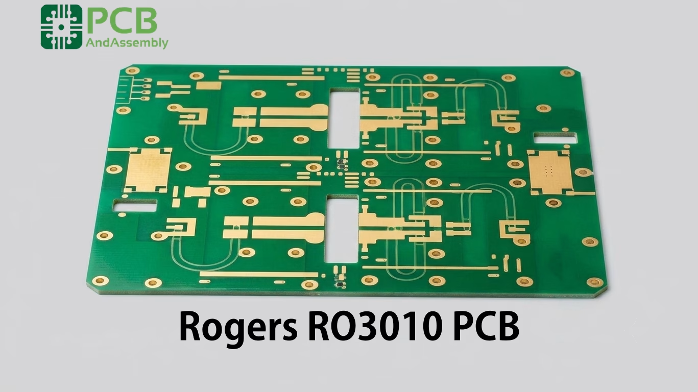
Table of Contents
- 1. What Is RO3010 PCB Material?
- 2. Electrical Characteristics
- 3. Mechanical & Thermal Properties
- 4. RO3000 Series Comparison
- 5. Standard Configurations
- 6. Fabrication Guidelines
- 7. Layout Design and Trace Geometry
- 8. Procurement and Cost Optimization
- 9. Key Applications
- 10. Frequently Asked Questions
- 11. Summary
1. What Is RO3010 PCB Material?
Rogers RO3010 is a ceramic-filled PTFE composite laminate built for commercial microwave and RF applications. It combines a PTFE matrix with ceramic fillers—delivering low electrical loss, tight dielectric tolerance, and strong mechanical stability in a single material.
Standard FR-4 fails above a few GHz. Its dissipation factor is roughly 10× higher than RO3010, and its dielectric constant (Dk) drifts significantly with both frequency and temperature. RO3010 solves these problems by design.
The ceramic filler does two jobs:
- Electrically: it raises the Dk to 11.20, compressing wavelengths and enabling significant circuit miniaturization.
- Mechanically: it stiffens the soft PTFE matrix, preventing cold flow and making the laminate compatible with standard PCB fabrication equipment.
Key Benefit: A Dk of 11.20 shrinks patch antennas, resonators, and transmission lines by more than 50% compared to FR-4 (Dk ≈ 4.3). This is critical for automotive radar, 5G arrays, and handheld RF devices.
Need PCB Manufacturing or Assembly?
Get a free quote within 24 hours. We specialize in prototype-to-production PCB/PCBA for hardware teams worldwide.
2. Electrical Characteristics
2.1 Key Electrical Properties
Table 1 lists the full electrical specification with design implications for each parameter.
| Property | Value | Test Method | What It Means for Designers |
| Process Dielectric Constant (Dk) | 10.20 ± 0.30 | IPC-TM-650 2.5.5.5 @ 10 GHz | Quality control / lot consistency check. Do not use this value in EM simulations. |
| Design Dielectric Constant (Dk) | 11.20 | Differential Phase Length, 8–40 GHz | Use this value in HFSS, ADS, and all impedance calculators. |
| Dissipation Factor (Df) | 0.0022 | IPC-TM-650 @ 10 GHz | Very low signal loss—reliable at mm-wave frequencies up to 77 GHz. |
| Thermal Coefficient of Dk (TCDk) | -395 ppm/°C | IPC-TM-650 2.5.5.5 | Dk stays stable across wide temperature swings—critical for filters and oscillators. |
| Thermal Conductivity | 0.62–0.79 W/m·K | ASTM C518 | Better than FR-4; supports heat dissipation in power amplifier designs. |
| Moisture Absorption | 0.05% | IPC-TM-650 2.6.2.1 | Prevents electrical detuning in humid, outdoor, or marine environments. |
| Volume Resistivity | 10⁷ MΩ·cm | IPC-TM-650 2.5.17.1 | Excellent electrical isolation, even under high-voltage bias. |
Rogers RO3010 PCB: Rogers RO3010 PCB Datasheet Download
2.2 Process Dk vs. Design Dk
RO3010 has two published Dk values. Understanding the difference is essential before you run any simulation.
Process Dk (10.20 ± 0.30): Measured by the clamped stripline method (IPC-TM-650) at 10 GHz. This is a manufacturing quality control number. It confirms lot-to-lot consistency—nothing more.
Design Dk (11.20): Derived from differential phase length measurements across 8–40 GHz. This accounts for copper surface roughness, dispersion, and dielectric-to-air interfaces at the microstrip boundary. Use this value in all EM simulators (ANSYS HFSS, Keysight ADS, etc.).
Warning: Using the Process Dk (10.20) instead of the Design Dk (11.20) in simulation will produce incorrect trace widths. This shifts filter center frequencies and creates impedance mismatches at ports.
2.3 Wavelength Compression and Miniaturization
The physical wavelength inside a dielectric follows:
λg = c / (f · √εeff)
At 10 GHz, raising Dk from 4.3 (FR-4) to 11.20 (RO3010) reduces the guided wavelength by more than 50%. Quarter-wave resonators, patch antennas, and power dividers all shrink accordingly. This matters most for:
- Automotive radar modules (77 GHz) fitted inside bumpers and grilles
- 5G small-cell antennas mounted on lamp posts and facades
- Handheld communication devices with tight PCB real-estate budgets
3. Mechanical & Thermal Properties
3.1 CTE Matching with Copper
Thermal expansion mismatch between a laminate and its copper cladding causes delamination, trace cracking, and via failures—especially under lead-free reflow profiles (peak 260°C) or automotive cycling (-40°C to +125°C).
RO3010 is engineered to match copper’s expansion closely in all three axes. Table 2 shows the comparison.
| Axis | RO3010 CTE (ppm/°C) | Copper CTE (ppm/°C) | Design Implication |
| X-axis | 13 | ~17 | Low mismatch—minimal lateral stress on traces. |
| Y-axis | 11 | ~17 | Low mismatch—consistent trace geometry after cycling. |
| Z-axis | 16 | ~17 | Near-perfect match—minimizes via barrel cracking and pad lifting. |
The Z-axis match is the most critical dimension. A large Z-axis CTE mismatch causes PTH barrels to expand faster than the surrounding dielectric during thermal cycling—leading to barrel cracks and pad lifts. RO3010’s Z-axis CTE of 16 ppm/°C sits very close to copper’s ~17 ppm/°C.
3.2 Moisture Resistance
Water has a Dk of approximately 80 at room temperature. Even small amounts of moisture absorption can shift a laminate’s effective Dk, detuning high-Q filters and altering transmission line impedance.
RO3010 absorbs only 0.05% moisture by weight. This makes it suitable for outdoor, marine, aerospace, and automotive deployments where humidity varies widely.
4. RO3000 Series Comparison
The RO3000 family shares consistent mechanical properties across all variants. This means you can mix different Dk values in a multilayer stackup without causing warpage or delamination. Table 3 shows the key differences.
| Parameter | RO3003 | RO3006 | RO3010 |
| Process Dk (10 GHz) | 3.00 ± 0.04 | 6.15 ± 0.15 | 10.20 ± 0.30 |
| Design Dk (8–40 GHz) | 3.00 | 6.50 | 11.20 |
| Dissipation Factor (10 GHz) | 0.0010 | 0.0020 | 0.0022 |
| X-Axis CTE (ppm/°C) | 17 | 17 | 13 |
| Z-Axis CTE (ppm/°C) | 24 | 24 | 16 |
| Best for | Ultra-low loss; wide traces | Moderate size reduction | Maximum miniaturization |
Choosing between variants comes down to one trade-off: miniaturization vs. loss. RO3010 delivers the highest Dk (most compact circuits) but slightly higher loss than RO3003. For designs where board area is the constraint, RO3010 is the right pick.
5. Standard Configurations
RO3010 is available in four standard thicknesses, two panel sizes, and multiple copper cladding options. Sticking to standard thicknesses reduces lead time and cost.
5.1 Standard Thicknesses and Applications
| Thickness (in) | Metric | Copper Options | Thickness Tolerance | Typical Application |
| 0.005″ | 0.13 mm | 0.5 oz (18 µm) or 1.0 oz (35 µm) ED | ± 0.0005″ | 77 GHz radar, ultra-compact mm-wave circuits |
| 0.010″ | 0.25 mm | 0.5 oz or 1.0 oz ED or Rolled | ± 0.0007″ | Microstrip and CPWG up to 40 GHz |
| 0.025″ | 0.64 mm | 1.0 oz (35 µm) or 2.0 oz (70 µm) ED or Rolled | ± 0.0010″ | Power amplifiers, couplers, high-power RF |
| 0.050″ | 1.28 mm | 1.0 oz or 2.0 oz ED | ± 0.0020″ | Antenna feed networks, rigid sub-assemblies |
5.2 Available Panel Sizes
- 12″ × 18″ (305 × 457 mm)
- 24″ × 18″ (610 × 457 mm)
- 24″ × 36″ (610 × 915 mm)
6. Fabrication Guidelines
Ceramic-filled PTFE requires process adjustments at several fabrication steps. A standard FR-4 line will produce defects if used without modification. Table 4 summarizes the key differences and the consequences of skipping them.
| Process Step | Standard FR-4 | Rogers RO3010 | Risk if Skipped |
| Drill Bit Selection | Standard carbide | Specialized high-grade carbide, optimized geometry, reduced spindle speed | Rapid wear → smearing → isolation of inner copper layers |
| Hole Preparation (Desmear) | Permanganate chemical desmear | Sodium naphthalene treatment OR plasma etching (He/O₂ or N₂/H₂) | Electroless copper cannot adhere → plating voids → open circuits |
| Lamination | 175–190°C | >200°C with specialized bondply cycles (e.g., Rogers RO4450 or high-Tg FR-4 prepreg) | Delamination, layer shift, board warp |
| Solder Mask | Standard LPI over all layers | Omit on RF signal paths; apply only on non-RF areas | Solder mask on RF traces → unpredictable Dk change → impedance shift |
| Material Pre-bake | Not typically required | 2–4 hours at 150°C to remove absorbed moisture before processing | Moisture-induced plating defects, lamination voids |
6.1 Drilling
The ceramic filler is highly abrasive. It wears standard carbide drills rapidly. Worn drills generate excess heat, causing the PTFE to melt and smear onto inner copper layers—creating open circuits.
Key drilling requirements for RO3010:
| Parameter | Recommended Value | Reason |
| Drill Speed | 200–300 SFM | Reduces heat buildup in abrasive ceramic-filled matrix |
| Feed Rate | 1.5–3.0 mils/rev | Controls chip load to prevent PTFE smearing |
| Retraction Rate | 500–1000 IPM | Clears chips before reentry |
| Stack Height | 2–3 panels maximum | Maintains drill bit accuracy and heat control |
- Use carbide drills with positive rake angles.
- Diamond-coated drills significantly extend tool life in high-volume production.
- Pre-bake material at 150°C for 2–4 hours before drilling to remove absorbed moisture.
6.2 Hole Wall Preparation (Desmear)
PTFE is chemically inert and hydrophobic. Electroless copper will not stick to an untreated PTFE hole wall. Standard permanganate desmear—used on FR-4—is ineffective on PTFE. You must use one of two alternatives:
Option 1 — Sodium Naphthalene Treatment:
A chemical solution that strips fluorine atoms from PTFE molecules at the hole surface, leaving a carbon-rich, hydrophilic layer that accepts copper plating.
Option 2 — Plasma Etching:
A dry vacuum process using He/O₂ or N₂/H₂ gas mixtures. Plasma bombardment chemically modifies the PTFE surface to allow adhesion. Typical treatment time is 10–20 minutes. This is the more commonly preferred method in modern fabrication.
Critical: Skipping hole wall preparation guarantees plating voids and via open circuits during reflow. Do not proceed to electroless copper deposition without one of these steps.
6.3 Multilayer Lamination and Hybrid Stackups
Hybrid stackups—RO3010 outer layers for RF routing, FR-4 inner layers for power and digital signals—are the standard cost-optimization approach. They work well when:
- High-frequency signals are confined to the outer layers
- Inner layers carry only DC power, control signals, or sub-GHz digital routing
- Bondply (e.g., Rogers RO4450) or high-Tg FR-4 prepreg is used to match thermal profiles
Because the RO3000 family shares consistent mechanical properties across variants, you can also mix RO3003, RO3006, and RO3010 in a single multilayer board without warpage or delamination issues.
7. Layout Design and Trace Geometry
7.1 Impedance Control on High-Dk Material
A high Dk compresses trace widths significantly. On a standard 0.010″ RO3010 substrate, a 50Ω microstrip trace is approximately 3.8–5 mils wide—depending on copper thickness and surface finish.
Narrow traces amplify the effect of etching variation:
- A 0.5-mil over-etch on a 3.8-mil trace (13% width reduction) shifts impedance by approximately 5Ω.
- A 5Ω impedance error causes measurable signal reflections and return loss degradation.
- At 77 GHz, even 2–3Ω of mismatch can degrade system noise figure.
Design practices that reduce sensitivity to etching variation:
- Use Coplanar Waveguide with Ground (CPWG) instead of microstrip where possible. The gap-to-ground on CPWG provides additional impedance control, allowing wider signal traces at the same target impedance.
- Include impedance test coupons on every production panel for TDR or VNA verification.
- Specify impedance tolerance as ±10% rather than ±5% unless the design requires tighter control. Tighter specs increase fabrication cost and reduce yield.
- Use Rogers’ free MWI (Microwave Impedance) Calculator for accurate line width modeling.
7.2 Transmission Line Structures
Three transmission line topologies are commonly used on RO3010:
Microstrip
Simplest to fabricate. The high Dk reduces radiation losses at mm-wave frequencies. Best for general-purpose microwave layouts.
Grounded Coplanar Waveguide (GCPW / CPWG)
Preferred for 77 GHz automotive radar. Provides tight ground return paths, reduces crosstalk, and allows wider signal traces. Better isolation than microstrip.
Stripline
Best isolation from external interference. Requires multilayer construction. Use for sensitive LNA inputs or high-isolation filter designs.
7.3 Copper Cladding: Surface Roughness
At mm-wave frequencies, the skin effect concentrates current at the surface of the copper trace. A rough copper surface acts as additional resistance, increasing insertion loss. The effect is frequency-dependent—roughness matters much more at 77 GHz than at 5 GHz.
| Copper Type | Surface Roughness (Rz) | Loss @ 30 GHz | Loss @ 77 GHz | Best Use Case |
| Electrodeposited (ED) | 2.0–3.0 µm | High | Very High | Cost-sensitive RF; lower frequencies |
| Low Profile (LP) | 1.0–1.5 µm | Moderate | High | Standard microwave up to 20 GHz |
| Rolled Treated | ≤ 0.5 µm | Very Low | Low | 77 GHz radar, mm-wave, high-sensitivity receivers |
7.4 Surface Finish Selection
Surface finish affects insertion loss on narrow, high-frequency traces. ENIG contains ferromagnetic nickel, which increases resistive loss at frequencies where the skin depth is shallow.
| Surface Finish | Loss Level | Recommended For | Notes |
| ENIG (Ni/Au) | High at mm-wave frequencies | Below 10 GHz or non-critical RF paths | Ferromagnetic Ni layer increases insertion loss via skin effect at high frequencies. |
| Immersion Silver (ImAg) | Low | 10–40 GHz microwave circuits | Preferred finish for critical RF traces on RO3010. |
| OSP (Organic Solderability Preservative) | Very Low | Cost-sensitive designs up to 40 GHz | Good RF performance; requires careful handling and storage. |
7.5 Via Design
Via performance becomes critical above 20 GHz. Follow these guidelines:
- Keep via aspect ratios below 8:1 for reliable plating.
- Use back-drilling to remove via stubs in thick multilayer boards—stubs cause resonance-related notches in the passband.
- Use via stitching around RF traces to maintain a continuous ground reference.
- Minimize via inductance in ground return paths; use multiple shunt vias where possible.
7.6 Ground Plane Design
- Use solid ground planes—avoid large cutouts under RF traces.
- Provide continuous ground reference under all transmission lines.
- For GCPW, ensure via stitching connects the coplanar grounds to the backside ground frequently.
8. Procurement and Cost Optimization
RO3010 costs significantly more than FR-4—typically 10–20× per panel. Expect $100–$600 per sheet depending on thickness and copper weight. Four strategies help manage this:
- Use Hybrid Stackups
Route RF signals on RO3010 outer layers only. Use FR-4 for all inner digital, control, and power layers. This is the single highest-impact cost reduction available.
- Stick to Standard Thicknesses
The 0.010″ and 0.025″ thicknesses are in stock at most qualified RF fabricators. Non-standard thicknesses force low-volume raw panel purchases, which increases unit cost and extends lead time.
- Optimize Panel Utilization
Rogers panels come in standard sizes (12×18″, 24×18″, 24×36″). Work with your fabricator early to nest boards efficiently. Unused raw panel area directly increases cost per unit.
- Specify Realistic Impedance Tolerances
A ±10% impedance tolerance is sufficient for most RF designs and is achievable without special process controls. Tightening to ±5% adds significant testing and yield cost. Only specify tight tolerances when the design actually requires them.
When RO3010 Cost Is Justified: Circuit miniaturization is a primary requirement · Operating frequencies exceed 30 GHz · Temperature stability over a wide range is critical · Long-term reliability in harsh environments is essential
9. Key Applications
9.1 Automotive Radar (77 GHz)
This is the fastest-growing application for RO3010. Modern ADAS systems use 77 GHz radar for adaptive cruise control, blind-spot detection, collision avoidance, and pedestrian detection.
At 77 GHz, the free-space wavelength is ~3.9 mm. Inside RO3010, it compresses to ~1.2 mm—enabling compact phased array antennas that fit behind bumpers and grilles. Vehicles must operate from -40°C to +85°C (and higher under the hood). RO3010’s stable Dk and copper-matched CTE ensure the radar performs reliably across thousands of thermal cycles over the vehicle’s lifetime.
9.2 5G Telecommunications
5G infrastructure demands high-frequency performance in compact form factors. RO3010 is used in:
- Massive MIMO base station antenna arrays
- Small cell units mounted on street furniture
- RF filters and couplers for 24–39 GHz mmWave bands
- Power amplifiers for base station transmitters
9.3 Satellite and Aerospace
RO3010 is used in direct broadcast satellite (DBS) converters, GPS antennas, airborne radar, and electronic warfare systems. Its low moisture absorption and stable Dk across temperature make it suited for airborne and space-adjacent environments.
9.4 RF Modules and Passive Components
Common module applications include:
- Patch antennas (70% smaller than FR-4 equivalent)
- Voltage-controlled oscillators (VCOs)
- Band-pass filters requiring stable center frequency over temperature
- Low-noise amplifiers (LNAs) and mixers
10. Frequently Asked Questions
Q: Why does the RO3010 datasheet list two different Dk values?
A: The Process Dk (10.20) is a quality control metric measured under clamped stripline conditions at 10 GHz. The Design Dk (11.20) reflects real-world microstrip operation across 8–40 GHz. Always use 11.20 in simulation and impedance calculations.
Q: What is the main difference between RO3010 and RO3003?
A: RO3010 has a Design Dk of 11.20 vs. 3.00 for RO3003. The higher Dk shrinks circuit dimensions by more than 50%—ideal for space-constrained designs. RO3003 offers lower loss and wider traces, making it better for wideband, low-loss applications where board area is not a constraint.
Q: How must RO3010 via holes be prepared before copper plating?
A: PTFE is chemically inert, so standard permanganate desmear will not work. You must use sodium naphthalene chemical etching or plasma treatment (He/O₂ or N₂/H₂) to activate the hole walls before electroless copper deposition. Skipping this step guarantees plating voids.
Q: Can RO3010 be used in multilayer boards with FR-4?
A: Yes. Hybrid stackups—RO3010 outer layers for RF routing, FR-4 inner layers for power and digital signals—are standard practice. Use Rogers RO4450 bondply or high-Tg FR-4 prepreg to bond the materials. This approach significantly reduces material cost without compromising RF performance.
Q: What surface finish should I use on RO3010 for mm-wave designs?
A: Immersion Silver (ImAg) or OSP are preferred on critical RF traces. ENIG contains a ferromagnetic nickel layer that increases insertion loss at frequencies where the skin depth is shallow (above ~20 GHz). Avoid ENIG on transmission lines operating above 10 GHz.
Q: What is the maximum operating frequency for RO3010?
A: RO3010 is reliably used at 77 GHz and beyond. The practical limit depends more on your design and fabrication capability than on the material itself.
Q: Is RO3010 compatible with lead-free soldering?
A: Yes. With a decomposition temperature (Td) of 500°C, RO3010 easily withstands lead-free reflow profiles peaking at 245–260°C. It also meets RoHS requirements and carries a UL 94 V-0 flammability rating.
Q: What is the typical PCB fabrication lead time for RO3010?
A: Expect 2–4 weeks for prototypes and 4–8 weeks for production quantities. Fewer PCB shops are qualified for PTFE processing, so establish supplier relationships early—before your schedule becomes critical.
11. Summary
Rogers RO3010 is engineered for one purpose: high-performance RF circuits where space, frequency, and reliability constraints leave no room for compromise.
Its four defining advantages are:
- Design Dk of 11.20 — enables the maximum circuit miniaturization in the RO3000 family
- Dissipation factor of 0.0022 — keeps insertion loss low from microwave to 77 GHz
- CTE closely matched to copper — protects traces and vias through thousands of thermal cycles
- Moisture absorption of only 0.05% — maintains stable RF performance in outdoor and harsh environments
Working with RO3010 requires specific adjustments: use the Design Dk (11.20) in all simulations, specify plasma or sodium naphthalene hole prep for all vias, choose ImAg or OSP over ENIG for mm-wave traces, and use hybrid stackups to control cost.
Follow these rules and RO3010 delivers exactly what it promises: compact, stable, and reliable RF performance at frequencies where no other practical material comes close.

Get Quote Free